Continue to Site

Welcome to EDAboard.com

Welcome to our site! EDAboard.com is an international Electronics Discussion Forum focused on EDA software, circuits, schematics, books, theory, papers, asic, pld, 8051, DSP, Network, RF, Analog Design, PCB, Service Manuals... and a whole lot more! To participate you need to register. Registration is free. Click here to register now.

Help! Can someone clarify to me how this converter circuit works?

Status
Not open for further replies.
It's ok. No problem. I still left about 1 month time to finish my project. Now I'm testing other parts leaving out the transformer part so that I do not need to rush.

So both LT1244 and UC3845 can use to regulate the circuit?
 

So both LT1244 and UC3845 can use to regulate the circuit?
Effectively yes..

The UC384X was originally introduced by a company called Unitrode, now owned by Texas Instruments, it has since been second sourced by others such as Fairchild, SGS Thompson and OnSemi. As well as that TI/Unitrode now produced an 'improved' range, the UCC380X devices. The Linear Technology device is their 'improved' version.

Linear Technology - LT1244 - High Speed Current Mode Pulse Width Modulators
http://cds.linear.com/docs/Datasheet/1241fa.pdf

http://www.onsemi.com/pub_link/Collateral/UC3844-D.PDF

The UC384X is effectively the 'jelly bean' current mode control SMPS integrated circuit rather like the 741/358/324 are, or were, for operational amplifiers.

In fact it looks like the version you will be using is going to become 'obsolete' but as suggested there are the newer part types available.

Genome.
 
Can I just use UC3845 since I had bought it?
By the way, I had tried checking the voltage across both capacitors in the forward converter. The input from the function generator is 5Vac and the max output I obtained is 7Vdc and drops back to 6.6Vdc, again back to 7Vdc. Is there any problem?
 

Well.. 5VAC is 5 x SQRT[2] peak or 7.07V. You might expect that you would lose some because of voltage drops in your rectifier diodes but since the currents being drawn will be low that forward drop need not be the 0.6-0.7V that is normally used. If you have the voltage balancing resistors in place then when the AC source drops below the output it no longer supplies current and the voltage will drop due to those resistors.

If you are using two capacitors in series along with two resistors then you can do some sums to see if things are reasonable.

Two capacitors, of the same value, in series look like one capacitor half the value. Your two resistors, of the same value, in series look like one resistor of twice the value. This is all that voltage divider stuff. Your resistors will draw a current from the capacitors and that current causes the voltage drop while your AC voltage is no longer charging the capacitors...

dV/dT = i/C

Since you are dealing with small changes you might assume that i will be constant. dT will be about 2/Fac as a result of the rectification. Grab your calculator and do some sums based on the component values and see if the 'approximate' answer agrees with what you are seeing in practice..

I've just updated the small signal model, the one being used for the AC/loop stability analysis, and found out my own sums on the switching model were slightly wrong, cough. I suppose it is always good to have a reality/sanity check. I'll update things later but at the moment Spice is being miserable.

Genome.

---------- Post added at 10:48 ---------- Previous post was at 10:37 ----------

Oooooops.

Theoretically yes you might use the UC3845 but its duty cycle is not limited to 50%. Remember that in this type of converter, the same as any other, you have to allow for the primary magnetising inductance to reset. Given it is set through VBUS and reset through VBUS then that results in your 50% duty cycle limit so it would be preferable to use an IC that gives that. I've ordered some UC3844's which are the right ones.

You might use the UC3845 but since its duty cycle extends to 100%, just below, then under transient conditions you might end up driving the transformer core into saturation at which point things might go BANG! The thing that would save the day is the fast current limit in the IC. If your layout is tight and you have used the right sort of sense resistor then it should catch that possibility and protect things. Not really something you should rely on but yes it is possible. Given there is an IC with the inherent limit in place then it is best to use it.

Genome.
 
Oh, sorry. It is my mistakes. I'm using 5Vpeak not 5Vac.

Yea, the voltage for each capacitor is around 3.4 to 3.5v.
 

Well, I've got 'all' the parts apart from the tape so I'll chase that up later on today.

Genome.
 
Tapes delivered. Packed up with rest of bits. Parcel is on the way.

Genome
 
... must try harder.

OK, bit of an oversight. I've previously stuck with the 50% duty cycle limit and designed the transformer to give about 48V out to achieve the final 24 volts. This is slightly wrong since it unbalances the available output inductor slew rate.

Going negative, with the primary side switches effectively off the inductor will be reset through 24V. Going positive with duty cycle at the maximum of 50% there is no voltage available to restore the inductor current and you end up with a 'sloppy' transient performance.


You'll see the error amplifier output has gone into positive limit with the filter inductor current in slew rate limit and the output being 'lazy' as it recovers. In order to get over that I've re-designed the transformer to give three times the required output or 72V. That will equalise things...


You are going to hate me but here is the transformer design...


.dxf file attached.

Next up the output filter inductor and hopefully a 'final' circuit diagram perhaps in time for when the bits arrive.

Genome.
 

Attachments

  • newtrans.zip
    3.4 KB · Views: 75
The filter inductor is a bit of a cheat given I have just picked another ETD29 core set but this time with a gap...

https://www.epcos.com/inf/80/db/fer_07/etd_29_16_10.pdf

The nice people at EPCOS also provide K factors for doing various calculations,


K1 and K2 are used to determine what sort of gap you would require for a particular Al value. For the inductor the minimum required turns are,

Nmin = L.Ipk/Bpk.Ae

L = 300uH
Ipk = 3A
Bpk = 0.3T
Ae = 76E-6

Nmin = 39

Since I have been chopping and changing things that has, sort of, gone out the window. I ended up buying sets of cores, one pair gapped to 0.2mm and the other to 0.5mm. If you put a 0.2mm one with a 0.5mm one then the total gap becomes 0.7mm

https://www.epcos.com/web/generator...ata__en.pdf;/PDF_ECoresGeneralInformation.pdf


Rearranging that gives Al = K1.S^K2 so with S=0.7 that gives Al = 159nH per root turn so I would need 43 turns for a 300uH inductor. Pick 40 as being bigger than the minimum 39 previously calculated and things will be near enough.

I'm quite surprised that one worked out so precisely. I'm sure I originally had a different answer... must be luck.

You should, some time, also have a reel of 0.85mm ECW which has an overall diameter of 0.9245mm and will, fingers crossed, give you 2 layers of 20 turns per layer for a total of 40 and you can use whichever pins you want for the terminations.

Genome.
 
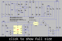
OK, after a bit of fiddling about and there will probably be some more this is the latest LTSpice model. Did I mention I am learning as well?


This time I have 'bit the bullet' and used the TL431 'properly' so the original secondary side operational amplifier has gone. In many respects I don't like the TL431 but they are widely used because the solution is 'cheap' but you spend a lot of time playing nursemaid to them... and opto-couplers. Of course maybe that is me.

I'll still have to generate and check an AC model for this. The way I have implemented it may introduce 'problems' elsewhere. It is a known effect that generating feedback with a TL431 operating off the rail it is regulating interferes with loop gain. I might be fairly sure that given the way I have used Q3/Q4 biased off the feedback chain is going to introduce similar effects.

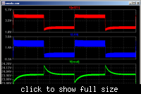
Anyway, the transient model says,


so things 'look' fairly spiffy.

Ignoring the overall compensation what I wanted to achieve is a standing current in both the opto-isolator and the TL431. In regulation the UC3844, or similar, will have its FB pin at 2.5V so with R16 at 510R the opto-isolator transistor will have to supply 4.9mA to get it there.

In this case I have used one of the available LTSpice models for a PC817A which has a current transfer ratio close to 100%. That means the diode will be driven at about 5mA which will be the current in the TL431 bringing it into its active range.

Being obtuse I have sent you a SFH610A-1 OPTOCOUPLER, TRANSISTOR O/P,

**broken link removed**

which has a CTR of 40%-80% @ 10mA so some components will have to be adjusted. A basic guess would be you double R16 and R14 and half C9. I've been mad for years. Then, in production, it would just be R17 that needs setting and things should iron themselves out.

One of the 'likes', and it may well be wrong, is that not only does the arrangement set up and more or less fix the required standing currents it also fixes the voltage levels on the opto-isolator transistor. Both the collector and emitter are 'pinned' at fixed voltages. That should maximise the devices bandwidth.

I might also claim that it does 'nice' things for the internal error amplifier of the control IC in terms of its gain-bandwidth product but that might be pushing things. My assumption is that it is effectively being run unity gain.

More words and an AC model later... You might need some data sheets for the bits I have sent.. I'll sort that later as well.

LTSpice model plus TL431 bits attached.

Genome.
 

Attachments

  • nmodb.zip
    7.2 KB · Views: 75
Hi, Genome.

In order to get over that I've re-designed the transformer to give three times the required output or 72V.
How the output 72V will drop to 24V since the pulse width is 50%.

According to the transformer design, I'm not really fully understand about winding to the margins and full width.
I also cannot open the transzip. Is it open by using LTspice?

Do you mean that for the 300uH inductor, the total winding is 40. So I should wind 20 per layer?
 

The maximum pulse width is 50%. The control IC adjusts that via feedback to regulate the output voltage. With 72V in and 24V out then in operation the pulse width will now, nominally, be 33%. It will vary as the input voltage varies, due to ripple or a line drop out, and under transient demands.

When you get the parcel you will find there are three reels of tape in it. Two are yellow 3M type 56 and one is white margin tape. You use the margin tape to fill in the edges of the bobbin by 4mm per side. This gives you the creepage and clearance distance and defines the portion in which the actual copper will fit.

You build the depth of that margin up gradually as you add the windings so for the first primary and primary auxiliary the depth of margin tape one side
would be sufficient for two layers of the 0.355mm ECW and the depth the other side sufficient for three layers.

When I say 'to the margins' that would use the narrower of the other two tapes just to cover the wire and stabilize things for winding the next layer. When I say 'full width' that would use the wider of the other two tapes to cover the wire and the margin tape.

I'm afraid my drawing wasn't overly explicit but things should become clear once you have the parts. Newtrans.zip contains a .dxf, Drawing Exchange Format file. It is a common format used for saving mechanical drawings produced by AutoCad and other drafting packages. You might be able to import it into your electronics package. Otherwise I've attached it as a .pdf file.

Genome.
 

Attachments

  • newtrans.pdf
    18.4 KB · Views: 85
Oh... forgot the last one. 40 turns would give you about 250uH. 43 would bring it up to the desired 300uH. The 'exact' value will not affect things too much as long as it is not ridiculously low or high.

In design terms the size of the inductor sets two things which are really related. One is the ripple current in the device.

dIout = VOUT.Toff/Lfilt

This, in conjunction with the output capacitor and its Equivalent Series Resistance, will determine the output ripple voltage or 'noise'.


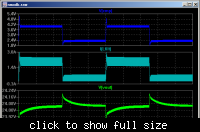
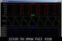
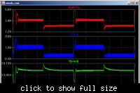
Top is the primary side gate drive, middle is ripple current in the inductor and bottom is ripple voltage on the output. The output capacitor should be selected to handle this ripple current,

:oops::oops::oops::oops:

https://www.farnell.com/datasheets/26036.pdf

Page 5)


I've gone and sent some 220uF 50V EEUFM1H221 devices and they are rated at 1650mA... Unfortunately they are going to be seeing 2000mA. It's not going to be 'explosive' but it will affect their lifetime. Nothing like getting it wrong to demonstrate how things should not be done...

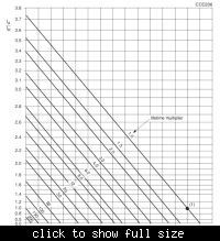
There are also 'multipliers' for such data. From Page 1),


Which, in this case, makes things slightly 'worse'. For better documented devices you will also get lifetime multiplier curves and a lot of other data.

https://www.soselectronic.hu/a_info/resource/a/pdf/rvi136.pdf


So whilst a device might be 'rated' for a lifetime of 4000 hours for example that is at the highest ambient temperature and with full ripple current applied. If you operate at lower ambient temperatures then it is possible to exceed the ripple current rating and still achieve a useful lifetime. That's assuming you have the qualifying data.

Obviously a lower ambient temperature means the device can dissipate more power in its ESR without its core getting as hot and as a result it will live longer.

I have digressed. One final thing about the ripple current is that as the output current demand from your supply falls you will reach a point when the inductor current becomes discontinuous..


That changes the gain characteristics of the loop. Whilst current is continuous the inductor 'integrates' the volt-seconds applied to it. When the current becomes discontinuous this no longer happens and that part of the loop goes from being first order to zero order. The supply may still be compensated to cope with that but things go slower as a result.

This is why some supplies need a 'minimum' current drawn from them to guarantee the specified performance or indeed remain stable.

For the moment I'm not overly concerned about getting the 'wrong' capacitor.

It is still going to do the job and, if more detailed information were available, then it is likely that given you will be operating at ambient temperatures lower than the 105C maximum rating things would actually be quite acceptable in terms of achievable lifetime.

Genome.
 
Last edited:
Thanks Genome. I'm more clear with the windings now.
For the regulating, do you mean that the regulator itself will change the pulse width when driving the MOSFET?

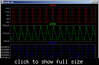
Genome, why the ripple current values for both pictures shown have so much difference? When will the inductor current be discontinuous?
 

Yes, that's the one. The internal error amplifier of the UC3844 along with the other components in the feedback loop will adjust the drive pulse width to the primary side switches in order to maintain the output voltage at 24V.

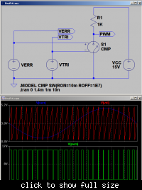
You may be used to 'voltage mode control' where the output of the error amplifier is compared to a 'ramp' waveform in order to achieve the pulse width modulation. I'm sure you have seen pictures like the following before,


Whilst the UC3844 does have a 'ramp' that is not specifically used for the pulse width modulation. It is there for timing and can be used for slope compensation. Otherwise for peak current mode control the 'ramp' used is that due to the ripple current in the output filter inductor reflected through the transformer onto the primary side and converted to a voltage across the current sense resistor..

The oscillator in the UC3844 is used to set a latch turning on the switches. When the sensed current exceeds that requested by the error amplifier it turns off the latch and therefore the switches. The overall result is pulse width modulation which acts to control the 'peak' secondary filter inductor current. Hence Current Mode control. Including slope compensation has the effect of making the circuit control average inductor current.

When the primary side switches are on, Ton, the output filter inductor is 'set' through the transformed primary voltage minus the output voltage and its current ramps up...

dIon = Ton.(VBUS/N - VOUT)/L

When the primary side switches turn off, Toff, current continues to flow in the inductor forcing the end connected to the rectifier and catch diode down to ground at which point the catch diode 'catches' it and holds it at 0V (-0.6V).

Now the inductor is being 'reset' through VOUT and its current ramps down

dIoff = Toff.VOUT/L

In regulation the average inductor current for a given load will be fixed so the amplitudes of those ramps has to be the same such that,

dIon = dIoff

and

Ton.(VBUS/N - VOUT)/L = Toff.VOUT/L

so

Ton.(VBUS/N - VOUT) = Toff.VOUT

If you normalise to one second then Ton is the operating duty cycle, D, and Toff becomes (1 - D)

D.(VBUS/N - VOUT) = (1 - D).VOUT

Multiply out,

D.VBUS/N - D.VOUT = VOUT - D.VOUT

Rearrange

D = N.VOUT/VBUS

For a non-isolated buck converter, the forward converter is part of that family the sum would have been,

D = VOUT/VIN

With the transformer in the way VBUS/N, with N being the turns ratio, is VIN so N/VBUS is 1/VIN and the equations are the same. The above however relies on the inductor current being 'continuous'. Ripple current in the inductor will be dIon, or dIoff since they are equal when inductor current is continuous. Using dIoff,

Iripple = (1 - D).VOUT/Fsw.L

If the load current drops below half that value then the inductor current will drop to zero during Toff, becoming discontinuous. At that point the catch diode turns off and its current will remain at zero until the next switching cycle begins. If the catch diode was replaced with a Mosfet and actively switched, synchronous rectification, then the inductor current would remain continuous but go negative.


V(CATCH,VOUT) is the voltage across the inductor. V(catch) is the voltage at the junction of the Rectifier and Catch diodes. When the inductor current falls to zero the catch diode turns off and V(catch) goes to VOUT placing zero volts across the inductor.

In the 'real' circuit you are likely to see a ringing waveform at that point, and it will happen elsewhere, due to parasitic capacitances in the circuit.

Genome.
 
Genome..For the converter circuit, is it necessary to use the resistor parallel to the capacitor. I had tested the circuit. There is large voltage drop from 5V to 1.4V. Can I just take off the 2 resistors and use 2 capacitors only?
 

It is 'advisable'. I'm not sure what your test set up is in terms of relative values but when the package arrives there will be some,

https://www.farnell.com/datasheets/86086.pdf

EEUEE2D101S 100uF 200V capacitors in there. From the data sheet,


Leakage current is specified as being "< 0.06 CV +10 (μA) After 2 minutes" so the expected maximum would be 0.06*100E-6*200 + 10uA or 1.24mA. You might hope that the devices are reasonably well matched, or just ignore it and 'hope' that any drift will be balanced, and pick 20% as a starting point which would be about 620K across each capacitor. It's not, or should not be something that will 'hurt' the final circuit.

What values are you testing with?

Genome.
 
I'm not sure how that would happen unless the signal generator you are driving your network with is unhappy about that particular load and going off to have a sulk as a result...

Genome.
 
Status
Not open for further replies.

Similar threads

Part and Inventory Search

Welcome to EDABoard.com

Sponsor

Back
Top