Continue to Site

Welcome to EDAboard.com

Welcome to our site! EDAboard.com is an international Electronics Discussion Forum focused on EDA software, circuits, schematics, books, theory, papers, asic, pld, 8051, DSP, Network, RF, Analog Design, PCB, Service Manuals... and a whole lot more! To participate you need to register. Registration is free. Click here to register now.

General IC footprint in ADS for double-sided boards

Status
Not open for further replies.

etmabreu

Full Member level 3
Joined
Mar 13, 2009
Messages
170
Helped
51
Reputation
102
Reaction score
49
Trophy points
1,308
Activity points
2,238
I have a problem while designing a PCB with Agilent ADS.

If one places a component, it is possible to flip it. But, unless as expected, the component footprint layer does not change from top to bottom (or vice-versa).

It happens that, if the component is flipped by mistake, there is no indication of such error!

Do you know how to overcome this in ADS?
 

ADS had no concerpt of top or bottom, it only considers layers. These layers can be in any order that the user chooses. It would certainly be possible to define layers to be used to define structures that are on the top and other layers that are define structure that are on the bottom. ADS does not know these relationships though, they are just layers.

Once you get to do EM then the substrate does define the stack-up of those layers once they are mapped there but just in the layout window there is no difference between the layers.

Some enterprise PCB component libraries do facilitate creating layouts that enable defining a SMT components to be place on the top or bottom side of the PCB but this requires specialist customization and capabilities to be embedded in the Design Kit that contains these components. It does not work with ADS components normally.

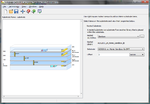
If you are using ADS 2012.08 then the suggestion there is that it should be possible to use the Nested Technology feature to embed Top and Bottom Technolgies for the surface mount components and to map one to the top and the other a flipped version to the bottom to produce this double sided style.

NestedSubstrates.png
 

Thank you very very very much for your reply!

Currently I am using ADS 2011.10.

I will explore "Nested technology" feature and come back to post results.

I was thinking in something very simple, such as having two layout views in the same cell and choose a correct one depending if the placed cell is fliped or not.
 

Status
Not open for further replies.

Part and Inventory Search

Welcome to EDABoard.com

Sponsor

Back
Top