Y.T_comp
Newbie level 6
hi all :-D
i have new question here:
i was reading in chapter 2 in mano book "digital design 2'end edition "
it was about gates delay in HDL .
he explain as normal this paragraph by an example which is :

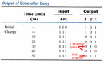
AND have 30ns delay ,OR 20ns and NOT 10ns .

and he side that the port X will go to it's final state after tow negatve spike or(20 nsec) .
so dose anyone know why he said that ?why X don't continue in its old state while this 20ns of delay end ?
thank you .
code of example is :
i have new question here:
i was reading in chapter 2 in mano book "digital design 2'end edition "
it was about gates delay in HDL .
he explain as normal this paragraph by an example which is :
AND have 30ns delay ,OR 20ns and NOT 10ns .
and he side that the port X will go to it's final state after tow negatve spike or(20 nsec) .
so dose anyone know why he said that ?why X don't continue in its old state while this 20ns of delay end ?
thank you .
code of example is :
Code Verilog - [expand]
Attachments
Last edited: