Continue to Site

Welcome to EDAboard.com

Welcome to our site! EDAboard.com is an international Electronics Discussion Forum focused on EDA software, circuits, schematics, books, theory, papers, asic, pld, 8051, DSP, Network, RF, Analog Design, PCB, Service Manuals... and a whole lot more! To participate you need to register. Registration is free. Click here to register now.

Gate drive for MOSFET bi-directional switch

Status
Not open for further replies.

Centmo

Member level 3
Joined
Mar 19, 2012
Messages
60
Helped
17
Reputation
36
Reaction score
17
Trophy points
1,288
Location
Canada
Activity points
1,772
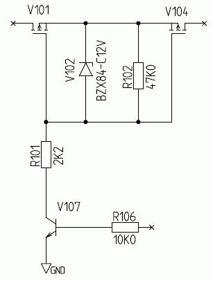
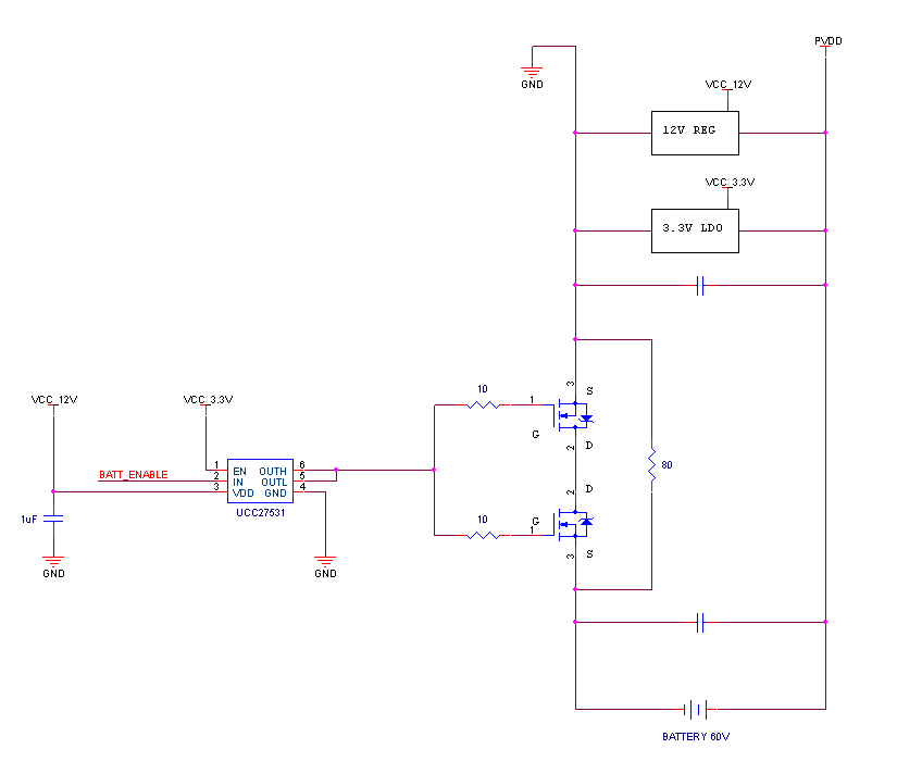
Hi, looking for some advice here. My system has two independent batteries connected, each with their own power-disconnect switch. Since current cannot be allowed to flow either way through the switch when off, two MOSFETs are used in a source-to-source configuration to create a bi-directional switch. My question is, how to achieve the gate drive of these FETs. They need to be able to be fully on (100% duty cycle) or off for extended periods of time. I don't expect that the attached schematic will work because the FET sources are floating when off. Note the 80ohm bypass which keeps the board MCU and voltage regulators powered even when the switches are off. Any suggestions?

Thanks.


You need isolation for the gate driver signal (e.g. by an optocoupler) and an isolated power supply. Or a level shifting driver designed specifically for the application.
 

If you want to use N-MOSFETS to switch the minus side of the battery to ground as you show, then you need an opto isolator to drive the gates, as FvM noted.

If you don't want to use a opto then you will need to use P-MOSFETs in a high side switch configuration. Note that the UCC27531 has a voltage maximum of 27V so you can't use that to drive the MOSFETS from an 80V supply.
 

I agree, PMOS makes things much easier. You can use a level shifting driver like below. The resistor values should be adapted to the supply voltage range.

8829614200_1393539382.gif
 
  • Like
Reactions: Centmo

    Centmo

    Points: 2
    Helpful Answer Positive Rating
Thanks for the replies. I think I have found a simpler solution (note that I have flipped the NFETs). In this design however, there cannot be a >6V difference across the switch. Unless perhaps if I put in a seperate 3V/12V supply and gate driver (and level shifter for BATT_ENABLE signal) for the low side.

Note: PFET is not as good for me due to high rds-on.

 
Last edited:

You're right, it's not very workable in that form. It's getting more complicated, but what about this?


The 80Ω resistor across the switches will carry up to an amp of current, even when the MOSFETs are off. It that okay?

What type of 3.3V and 12V regulators are you using that can tolerate 80V on their inputs?
 

Can work, but incredibly complicated.

You can design a level shifter similar to post #4 for NMOS. Needs a positive (e.g. +12V) supply and a second driver transistor because the gate level ranges between -60 and a positive Vgson value.
 

After some thought I realized that you don't necessarily need an opto isolator since the 80Ω bypass resistor provides a path for the control current. Below is a circuit that uses a high voltage NPN and PNP to control the MOSFETs gate voltage. The zener prevents the Vgs from exceeding 12V.

Low Side Driver.gif
 
Last edited:
  • Like
Reactions: Centmo

    Centmo

    Points: 2
    Helpful Answer Positive Rating
Also without the 80 ohm resistor, you don't need optocouplers. But a positive supply connected to Q2 emitter.
 

The 80Ohm bypass is required to power the MCU and other electronics when the switches are turned off to both batteries (which is the starting condition). Note that when turned on, the switch will carry over 100A. For the 12V supply, I found the TPS7A4001 (up to 80V input). From this 12V supply, I can drive a 3.3V regulator (not shown this way in my schematic).

Note that since there are two such batteries connected in the same way, it needs to operate safely when the batteries are at different voltages. This was the reason for the optoisolator for the control signal in the drain-to-drain configuration of post#7. If the PCB is at 55V due to connection to the other battery not shown, and the battery shown is 60V and not switched in, then there would be a 5V delta across the 80ohm, and the control signal would not be a suitable voltage for the lower NFET.

crutschow, that is an interesting circuit, do you know if it has been tested in real life? I am trying to figure out how the gate charge current makes it's way back to the battery if the NFET is off (KCL). By leakage current? This could mean a slow turn-on time depending on the FET properties?

FvM, your circuit looks like the same idea. I suppose a large-value resistor could be added between the source-source point and the battery ground to provide a better gate charge current path.

I'm going to study this circuit further.
 

crutschow, that is an interesting circuit, do you know if it has been tested in real life? I am trying to figure out how the gate charge current makes it's way back to the battery if the NFET is off (KCL). By leakage current? This could mean a slow turn-on time depending on the FET properties?

FvM, your circuit looks like the same idea. I suppose a large-value resistor could be added between the source-source point and the battery ground to provide a better gate charge current path.
The circuit doesn't depend on leakage currents or additional resistors. The gate driver is always operational by effect of the MOSFET substrate diodes.

I think you can easily verify the circuit operation under different battery conditions with a circuit simulator.
 
  • Like
Reactions: Centmo

    Centmo

    Points: 2
    Helpful Answer Positive Rating
The circuit doesn't depend on leakage currents or additional resistors. The gate driver is always operational by effect of the MOSFET substrate diodes.

I think you can easily verify the circuit operation under different battery conditions with a circuit simulator.

Yes I see now, through the body diode.

- - - Updated - - -

Also, I suppose turn-on and turn-off time can be adjusted by changing the resistor values R1 and R2 of the diagram in post#10. It is quite a simple circuit.
 

.....................................
crutschow, that is an interesting circuit, do you know if it has been tested in real life? I am trying to figure out how the gate charge current makes it's way back to the battery if the NFET is off (KCL). By leakage current? This could mean a slow turn-on time depending on the FET properties?

........................
I have not tested it, only simulated it.

The gate charge capacitor is dissipated by R2 to the sources.
 

Status
Not open for further replies.

Similar threads

Part and Inventory Search

Welcome to EDABoard.com

Sponsor

Back
Top