Continue to Site

Welcome to EDAboard.com

Welcome to our site! EDAboard.com is an international Electronics Discussion Forum focused on EDA software, circuits, schematics, books, theory, papers, asic, pld, 8051, DSP, Network, RF, Analog Design, PCB, Service Manuals... and a whole lot more! To participate you need to register. Registration is free. Click here to register now.

Gain expansion

Status
Not open for further replies.

junhao

Junior Member level 2
Joined
Aug 13, 2021
Messages
20
Helped
0
Reputation
0
Reaction score
0
Trophy points
1
Activity points
145
嗨,我在设计功率放大器时看到了 5dB 的增益扩展,栅极电压显示 MOSFET 在深度 AB 类中工作。我不希望这种增益扩大,但我不知道如何减少这种现象。请问你能帮帮我吗?

[Betwixt] For the benefit of non-Chinese speakers, it translates as:

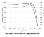
Hi, I saw a gain extension of 5dB when designing a power amplifier, and the gate voltage shows that the MOSFET is working in deep class AB. I don't want this gain to expand, but I don't know how to reduce this phenomenon. Could you please help me?
 
Last edited by a moderator:

Gain expansion is pretty much unavoidable in a class-AB amplifier.
Placing the PA bias near class-A, the gain expansion will be minimized.
 

Are you talking about 5dB extra voltage gain when both class-AB output transistors conduct at crossover? Emitter-followers don't do it because their gain is never more than 1.

If you have a Mosfet pair operating as common-source instead of as followers then the amplifier's negative feedback should reduce the extra gain at crossover.
 

Gain expansion is pretty much unavoidable in a class-AB amplifier.
Placing the PA bias near class-A, the gain expansion will be minimized.
Yeah, I have increased the DC bias, while this phenomena didn't get better, and I check the active voltage of MOSFET, just as the picture shows, I think it's still in deep CLASS AB.
 

Attachments

  • 901cb942bc465db1ffefd20a45b2569.jpg
    901cb942bc465db1ffefd20a45b2569.jpg
    5 MB · Views: 109
  • fc582e5cbc73c0ec947912854ae553f.jpg
    fc582e5cbc73c0ec947912854ae553f.jpg
    2.1 MB · Views: 119

h class-AB output transistors conduct at crossover? Emitter-followers don't do it because their gain is never more than 1.
If you have a Mosfet pair operating as common-source instead of as followers then the amplifier's negative feedback should reduce the extra gain at crossover.

Are you talking about 5dB extra voltage gain when both class-AB output transistors conduct at crossover? Emitter-followers don't do it because their gain is never more than 1.

If you have a Mosfet pair operating as common-source instead of as followers then the amplifier's negative feedback should reduce the extra gain at crossover.
I got a inductor at source of transistor while it has a little effect. And the OP1dB, gain decreased a lot.
 

I think is about an LDMOS PA. LDMOS have AB-class gain expansion higher than other technologies.
If increasing the bias doesn't help much, the only thing that remain is to do a larger back-off power.
Gain expansion may affect the phase change during expansion, so is good to increase the PA bias or to do the power back-off just to pass those phase change system requirements.
 

Attachments

  • AB.jpg
    AB.jpg
    85.2 KB · Views: 96

Gain expansion occurs when the Input Signal Amplitude starts to shift the Bias Point of the Amplifier ( especially the last stage of a Chain ) through increment sense .In order to overcome this phenomena, Bias Voltage can be adjusted according to Output Power like Envelope Tracking.It's a bit complicated but efficient.
 

I think is about an LDMOS PA. LDMOS have AB-class gain expansion higher than other technologies.
If increasing the bias doesn't help much, the only thing that remain is to do a larger back-off power.
Gain expansion may affect the phase change during expansion, so is good to increase the PA bias or to do the power back-off just to pass those phase change system requirements.
1dB gain expansion is acceptable, while 3 or 5dB is too terrible.
 

Gain expansion occurs when the Input Signal Amplitude starts to shift the Bias Point of the Amplifier ( especially the last stage of a Chain ) through increment sense .In order to overcome this phenomena, Bias Voltage can be adjusted according to Output Power like Envelope Tracking.It's a bit complicated but efficient.
Yeah, I agree. But this phenomena appears in 2nd driver stage, and it's a cascode structure with three transistors stack, and the voltage swing is extremly large between the middle of the three transistors, I haven't fingured out the reason. Generally, the transistor which connects to the VDD directly suffers the largest voltage swing.
 

I think is about an LDMOS PA. LDMOS have AB-class gain expansion higher than other technologies.
If increasing the bias doesn't help much, the only thing that remain is to do a larger back-off power.
Gain expansion may affect the phase change during expansion, so is good to increase the PA bias or to do the power back-off just to pass those phase change system requirements.
Could you explain how does gain expansion affects the phase change please? I found that decreasing the gate voltage made the gain expansion improved and also AM-PM got better.
 

Any linear active device when goes in compresion (non-linear mode) starts to affect the AM-PM response.
A main cause of AM-PM effects appears to be the dynamic mistuning of the input match.
The reason that you get better AM-PM response for less gate voltage might be because the gain of the PA is lower.
Yeah, the gain of PA decreases about 2dB, I think the swing is too large which can reach 0.5V~6V, it may cause the CS transistor achieve linear region or deep triode region, while the input match isn't perfect conjugate match, then the current's phase caused by drain voltage is different from caused by gate voltage, so the AM-PM curve is about 8°/dB. I don't konw this idea whether right or wrong.
 

Any linear active device when goes in compresion (non-linear mode) starts to affect the AM-PM response.
A main cause of AM-PM effects appears to be the dynamic mistuning of the input match.
The reason that you get better AM-PM response for less gate voltage might be because the gain of the PA is lower.
I also wonder that does this phenomenon is related to the transconductance of large signal. Maybe third-order transconductance?
 

Status
Not open for further replies.

Part and Inventory Search

Welcome to EDABoard.com

Sponsor

Back
Top