Continue to Site

Welcome to EDAboard.com

Welcome to our site! EDAboard.com is an international Electronics Discussion Forum focused on EDA software, circuits, schematics, books, theory, papers, asic, pld, 8051, DSP, Network, RF, Analog Design, PCB, Service Manuals... and a whole lot more! To participate you need to register. Registration is free. Click here to register now.

Fully differential current-steering DAC structure

Status
Not open for further replies.

user0088

Junior Member level 3
Joined
Dec 30, 2011
Messages
30
Helped
0
Reputation
0
Reaction score
0
Trophy points
1,286
Activity points
1,467
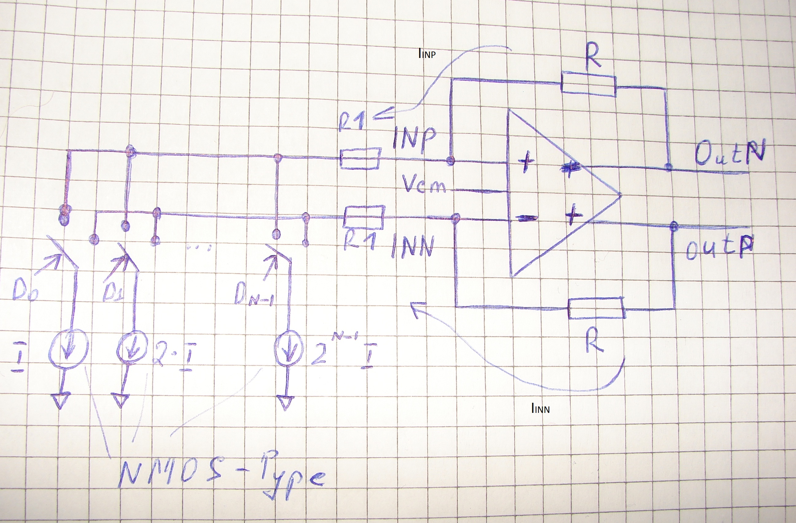
Please help in providing some information/document for fully differential current-steering DAC structure.
I mean a structure, where after current sources a fully differential amplifier is used, which outputs vary over common-mode voltage (both up and down directions).

In a case of using structure shown in attached file, both outputs of a differential amplifier (OUTP and OUTN) will always be below from some common-mode voltage, independent on the input digital code (D0,D1,...).

Current_Steering_DAC.JPG

So, how to have a fully differential outputs? I have searched a lot, but I haven't found any helpful information.
I think, that both PMOS and NMOS types current sources can be used for this purpose, but.......I guess the mismatches will greatly effect on DAC performance.

I want to know how is getting fully differential current-steering DAC in practice.

Thanks in advance.
 

In a case of using structure shown in attached file, both outputs of a differential amplifier (OUTP and OUTN) will always be below from some common-mode voltage, independent on the input digital code (D0,D1,...).

No. The common mode path of a fully differential amplifier will enforce (Voutp+Voutpn)/2 = Vcm.

The amplifier polarities are drawn wrong, by the way.
 

No. The common mode path of a fully differential amplifier will enforce (Voutp+Voutpn)/2 = Vcm.

Could you please explain this in more detail?

The amplifier polarities are drawn wrong, by the way.

You mean that INP should be connected to OUTN, and INN to OUTP ?
 

You mean that INP should be connected to OUTN, and INN to OUTP ?
Yes, otherwise the feedback resistors don't work.
Could you please explain this in more detail?
I'm referring to usual fully differential amplifiers, that include a common mode feedback path. It's discussed in analog IC design text books, e.g. Gray/Hurst/Lewis/Meyer, Analysis and Design of Analog Integrated Circuits, Chapter 12. I don't know the features of your differential amplifier.
 

FvM, thanks for your replies.

But it is not clear for me. Is it possible with only one type current sources (nmos type, in the example in my first post) and fully differential OA usage to get a fully differential DAC, which outputs (OA outputs) vary over common-mode in both directions, i.e. for example, INP can have a (CM+Vdelta) and (CM-Vdelta) values, where Vdelta is a input code based voltage, CM=const=VDD/2.

Thanks in advance.
 

Is it possible with only one type current sources (nmos type, in the example in my first post) and fully differential OA usage to get a fully differential DAC, which outputs (OA outputs) vary over common-mode in both directions.

It depends on the input common range of amplifier and current source voltage range.
 

I worked on capacitor binary array circuits but as far current sources are concerned,
Criteria is, available overdrive voltage, Voltage range you have available and finally, your current source matching and noise response.
You have to decide what is best?
 

It depends on the input common range of amplifier and current source voltage range.

is it possible with the scheme attached in the first post as well (assume, that INP connected to OUTN, and INN to OUTP) ??? please not that only nmos type current source is used.
 

is it possible with the scheme attached in the first post as well
The most negative amplifier output voltage can't swing below the input common mode range and current source output voltage range. Depending on the intended output voltage range it may work.
 

The most negative amplifier output voltage can't swing below the input common mode range and current source output voltage range. Depending on the intended output voltage range it may work.

So, how to have a fully differential outputs? I mean, that both OA outputs (OUTP and OUTN) could vary from 0.1*VDD to 0.9*VDD, whereas input common voltage is 0.5*VDD.

Thanks in advance.
 

So, how to have a fully differential outputs? I mean, that both OA outputs (OUTP and OUTN) could vary from 0.1*VDD to 0.9*VDD, whereas input common voltage is 0.5*VDD.

Thanks in advance.

Yes. that is how an op-amp works. Due to high open loop gain (theoretically infinite) with resistive feedback would force your inp and inn to be equal to the common mode value. the output common mode will be set based on the common mode feedback voltage. when you steer the current the output would swing based on CurrentSteered*Resistance.
 

when you steer the current the output would swing based on CurrentSteered*Resistance.

steadymind,
Let's assume that we use ONLY nmos-type current source(see fig in the first post, assume, that INP connected to OUTN, and INN to OUTP).
Let's assume that input digital code is 11111....11111. So, the whole current goes, from example, ONLY through INP.
So, OUTN will be (CM-CurrentSteered*Resistance). Is it so? But how OUTP will be (CM+CurrentSteered*Resistance) ?????????????? if no current goes through INN ???
Could you please explain. Thanks.
 

You need to have another resistor between INP and the node connecting the current switches. That will help setup virtual ground (CM at inputs). In other words you need to have a DC bias condition.
 

You need to have another resistor between INP and the node connecting the current switches. That will help setup virtual ground (CM at inputs). In other words you need to have a DC bias condition.

Is it possible to have a fully differential outputs with the attached circuit ???
 

Can someone please show practical implementation of fully differential current-steering DAC. It is not clear is it possible with the circuit shown in #14 to have an OA outputs (OUTP and OUTN) which could vary from 0.1*VDD to 0.9*VDD (input common voltage is 0.5*VDD).

Help me Please.
 

Can someone please show practical implementation of fully differential current-steering DAC. It is not clear is it possible with the circuit shown in #14 to have an OA outputs (OUTP and OUTN) which could vary from 0.1*VDD to 0.9*VDD (input common voltage is 0.5*VDD).

Help me Please.

have a look at this
https://ieeexplore.ieee.org/xpl/articleDetails.jsp?tp=&arnumber=5770757&contentType=Conference+Publications&searchField%3DSearch_All%26queryText%3Ddifferential+current+steering+DAc
 

Status
Not open for further replies.

Similar threads

Part and Inventory Search

Welcome to EDABoard.com

Sponsor

Back
Top