Continue to Site

Welcome to EDAboard.com

Welcome to our site! EDAboard.com is an international Electronics Discussion Forum focused on EDA software, circuits, schematics, books, theory, papers, asic, pld, 8051, DSP, Network, RF, Analog Design, PCB, Service Manuals... and a whole lot more! To participate you need to register. Registration is free. Click here to register now.

Full Bridge with vin = 200Vdc and no Gate zeners

Status
Not open for further replies.

cupoftea

Advanced Member level 5
Joined
Jun 13, 2021
Messages
2,653
Helped
54
Reputation
108
Reaction score
116
Trophy points
63
Activity points
13,956
Hi,
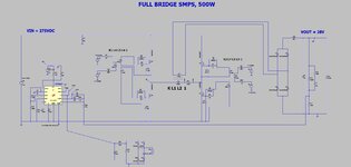
Just seen a Full Bridge with Vin = 200Vdc. (output of 115VAC PFC)
Fsw = 47kHz.
Its gate drive is two pulse transformers each with 2 secs........for each leg......bipolar drive....in each secondary is only a 12R series resistor and 12k gate_source res.
No gate zener (back to back)
Would you think this was unadviseable?
 

This can easily work - esp if each Tx drives a diagonal pair of devices - i.e. both on or both off

this little trick has been around for a long time ...
 
Thanks, my apologies, i was only referring to the lack of back to back protection zeners as being unadviseable?

I appreciate the gate drive method is good.
(even though gate drive voltage level depends on duty cycle, and also its not so easy to get good interleave winding done as with a single fet pulse transformer drive...also, the PCB tracking from pulse txformer to one of the fets can end up being longer than a single pulse txformer serving each fet....but otherwise is good)
 
Last edited:

GD level does not have to be tied to duty cycle - for a bridge driven GD tx, or or the fwd driven GD TX driving a diagonal pair ....
--- Updated ---

zeners not needed - only for GD Tx's with a lot of leakage and long lines to the G-S ...
 

zeners not needed - only for GD Tx's with a lot of leakage and long lines to the G-S ...
Thanks, in that case i'd say they (back to back zeners) are needed for us. Our GDT is just three coil, no sandwich winding. And tracking to the fet near the txformer is short, but long to the other of the leg pair.

Also, this gate drive method cant use Turn off PNP.s...seems not so good.

GD level does not have to be tied to duty cycle - for a bridge driven GD tx, or or the fwd driven GD TX driving a diagonal pair ....
Thanks, though ours is the simplest rendition of it....and so voltage drive level varies with duty.
AYK, for the secondary coil.....V.dt on must equal v.dt off.....as such, as you well know, the voltage drive level varies with duty.
But thanks, and I am appreciate you will have a better way to do it than this.
 

The "goodness" of gate drive is closely linked to power level - for 10W you can get away with a lot, for 100W it needs to be a bit better,

for 1kW, it needs to be designed and laid out by engineer with > 10 years experience

for 2kW + and higher freq - you need the best ...
--- Updated ---

p.s. you state bipolar drive and full bridge converter, so 0 - 48% on time

surely the GD level is constant then ...? ( GD Tx saturating ? causing droop, too small cap in series with GD Tx ? )
 
too small cap in series with GD Tx
Thanks.....there's a cap in series with the single pri.....but no cap in series with the two secondaries that are on the same core.
 

for 1kW, it needs to be designed and laid out by engineer with > 10 years experience
Thanks, well ours is half that power, and just uses one of these pulse transformers for each leg..
B82804A0264A210
fsw is 47kHz.
The primary just has a series cap...and the secondaries.... each has no more than a series 12R, and shunt 12k...thats it.

..Personally i would have done DC restoration in each sec...then PNP turn off.
 

From data sheet, 22V.us, 47kHz, 10 uS each way, thus 2.2 volts, thus the GD Tx is saturating, thus the volts are drooping after 2.2uS approx ( for 10V )

thus - you need a bigger GD Tx ....
 
My sincere Apologies,,,,this schem is horrendous, there are RC timing components on the schem, then the component identifys different when you click, then on the BOM its different again. The switching frequency now is coming out, for this Full bridge, as 450kHz, rather than 47kHz. Its UC2825 with rt = 6040R and ct = 560p. Again my sincere apologies.
The gate drives appear to have been connected up as if its a PSFB, but its not a PSFB driver.
...Just unpicking it all now.
 
Last edited:

Thanks Easy Peasy, you were correct in your other post......their SMPS design is appalling and we need to dis-associte from it. Shame because this was to be a good payer......but must drop it and go back out onto the market now.
I show it here in jpeg and LTspice. I am going to have to tell them its no good. (its certainly not worth keeping secret as you will know)
For some reason they seem to want to move forward anyway.
(the attached is a rep only....the actual uses UC2825)
They have the bizarre gate drive as shown which means the fets dont get much of a drive voltage, and also the fets arent actually properly held off for much of the switching period...and also they cant do more than 0.5 duty cycle....not good as the leakage L can mean you need more duty cycle than the ideal calcs.
They also have slow gen purpose diodes across their bridge fets, whose internal diode has trr=500ns.
Also, Bridge output uses 400V UF diodes..instead of 100V schottkys with RC snubbers.
The 450kHz switching frequency for a 500W hard switched full bridge switching off 275vdc sounds bad too.
The RM12 has no creepage or tubing, just plain enamelled copper wire for pri and sec. No margin tape.
The 12V Vcc to the UC2825 is not even a reg'd 12V....its a secondary of a flyback whose aux output is regulated. The Aux flyback FET would get smashed by the reflected voltage. Its 20:1 (275vin, 12vout). Flyback FET is 450V.
Again, only decoupler on the 275VDC is the 5 series axial tantalums.

May i ask, has anyone ever seen this gate drive method for a Full Bridge? What was the circumstances?
 

Attachments

  • Full Bridge BAD GATE DRIVE.jpg
    Full Bridge BAD GATE DRIVE.jpg
    148.3 KB · Views: 84
  • Full Bridge _BAD GATE DRIVE.zip
    3.3 KB · Views: 88
Last edited:

Thanks, yes sorry , i am mistaking the gate drive method in #11 for one i saw in a different product....the gate drive method we have is actually good, and doesnt reduce voltage with duty, but has no back to back zeners. and no clamping for leakage L ringing voltage. As such, this must be a very bad idea for a 500w full bridge converter?
 

Status
Not open for further replies.

Part and Inventory Search

Welcome to EDABoard.com

Sponsor

Back
Top