Continue to Site

Welcome to EDAboard.com

Welcome to our site! EDAboard.com is an international Electronics Discussion Forum focused on EDA software, circuits, schematics, books, theory, papers, asic, pld, 8051, DSP, Network, RF, Analog Design, PCB, Service Manuals... and a whole lot more! To participate you need to register. Registration is free. Click here to register now.

Full Bridge Unfolding Cicuit

Status
Not open for further replies.

Ashvinpambhar

Newbie level 5
Joined
Nov 17, 2019
Messages
9
Helped
0
Reputation
0
Reaction score
0
Trophy points
1
Activity points
99
Hi,
I used a controller dsPIC33FJ16GS504 for on gird solar-microinverter, in my hardware part when I applied input (24-dc battery not a solar panel), also connect lamp of 300 W as a load, and applied a grid to the output side as per given in document (for detail microchip document AN1444).
I also read a procedure to start hardware. As per procedure first step connect grid and load then start power on switch which is connected between battery and input.
My question is that when I start a power on switch after completing a procedure as per above, a part of hardware known as a full bridge unfolding circuit (attached with this post and also available on document AN1444 page no 11) has a four MOSFET (IPB60R190C6) in which only right top MOSFET is burn out after some time (1 to 2 minutes) and remaining three has no effect like that. So my problem is why only one MOSFET (top-right) is burn out not other and what is the solution for that. (for detail circuit description given in document AN1444).
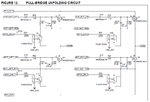
1.png
 

Hi, You should not drive Full Bridge FETs like that.....the opto wont be able to pull enough current , and its response wont be quick enough.
Use either a Bootstrap high side driver IC , or a pulse transformer.
 

Hi,
I used a controller dsPIC33FJ16GS504 for on gird solar-microinverter, in my hardware part when I applied input (24-dc battery not a solar panel), also connect lamp of 300 W as a load, and applied a grid to the output side as per given in document (for detail microchip document AN1444).
I also read a procedure to start hardware. As per procedure first step connect grid and load then start power on switch which is connected between battery and input.
My question is that when I start a power on switch after completing a procedure as per above, a part of hardware known as a full bridge unfolding circuit (attached with this post and also available on document AN1444 page no 11) has a four MOSFET (IPB60R190C6) in which only right top MOSFET is burn out after some time (1 to 2 minutes) and remaining three has no effect like that. So my problem is why only one MOSFET (top-right) is burn out not other and what is the solution for that. (for detail circuit description given in document AN1444).
View attachment 157093

I have seen this circuit but went my own way with a completely different drive design however I can tell you a few reasons why unfolder mosfets fail! Firstly overvoltage, I don't know if you have implemented the full line filter given in the app note but if not it would be a good idea to do so as it helps to suppress grid born spikes, additionally I fitted 1K5 TVS diodes across each mosfet it is however difficult to select the voltage to both protect the mosfet and have enough standoff.

The second reason is timing including software bugs or bad zero cross detection, this can cause the unfolder to turn on at other than true zero-cross or even worse in grid antiphase causing very high peak currents destroying the mosfets.

The nature of the beast being at high voltage makes debugging difficult and potentially dangerous, please be careful.

PS I don't like the drive circuit either as being AC transformer coupled the turn on is very slow. I don't know to what extent microchip rigorously tested it in real life, I suspect maybe not.........

Having thought about this a bit more I think I have seen that AC drive circuit before in a thyristor based unfolder (the AC is of course turned on/off) they appear to have adapted it not very well to mosfets by adding the opto-coupler to try improve turn-off timing. You will have to confirm this by combing through the software (is the AC modulated) IMOP the arrangement sucks!!
 
Last edited by a moderator:
  • Like
Reactions: FvM

    FvM

    Points: 2
    Helpful Answer Positive Rating
Hi, You should not drive Full Bridge FETs like that.....the opto wont be able to pull enough current , and its response wont be quick enough.
Use either a Bootstrap high side driver IC , or a pulse transformer.

actually, opto-coupler's CTR (current transfer ratio) capability is 300 to 600 % and as per datasheet its frequency response is upto 80khz. its rise time and fall time in 18 microsecond maximum. actually, i used this opto-coupler for providing a discharge path to the MOSFET, no any other used of opto-coupler.
here i used MOSFET's switching frequency is 228 kHz bus opto-coupler's switching frequency is upto 100 to 120 Hz only.
For detail explanation please refer document AN1444.
 

A FET driver (which you have not shown in the schem) should always have a very low output impedance so it can put the short high current pulse into the mosfet gate so as to turn it on/off.....so i assume your fet drivers are like that............you seem to be shorting the output of your fet driver via those optos......that is not a good idea.
 

Status
Not open for further replies.

Part and Inventory Search

Welcome to EDABoard.com

Sponsor

Back
Top