Darktrax
Full Member level 5
Going into new ground for me, I seek hints on how to handle what looks like difficult choices when it comes to using circuit board substrates and surface mount packages at 10Ghz, without going into alumina hybrids and flip-chips. The device I have in mind is NE3511S02, but the same considerations apply to almost any microwave transistor.
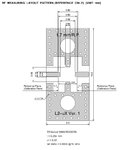
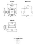
The vendor information footprint used for s-parameter measurements is on 0.254mm (10mil) glass-PTFE Rogers 5880, about the thinnest available. It is soft stuff, hard to plate without sodium etch, has 50-Ohm lines 0.74mm wide.
There is a via directly under the package source connections, which is a no-no for reflow solderpaste soldering.


The first thing I did was EM simulate the half-footprint attached to a source to discover the inductance of the set of vias, which includes one huge hole, leading to the question.. do single larger diameter vias lower the inductance faster than lots of tiny vias in parallel?
GIven there are 2 source tabs connected together, might there be a reason for having the underside clear, instead of placing a track right through between source pads, possibly helped by a via or two?
For design stability, we need a special amount of inductance in the source connection.
More - I want to make the substrate thicker - say 0.762mm (30 mil), in Er=3.5, where the 50 Ohm strips are 1.68mm wide, using a substrate (Taconic) where the strip loss is kept low from good underside surface finish.
Right now, it is making new via layouts that give that extra 100pH over the approx 30pH the vendor reference has, making new footprints that fit the strip widths for thicker board, and wondering how far I can mess with it before invalidate the s-parameter set.
I feel I may be knocking myself out doing stuff the hard way, but I can see no other good way. Advice from any who have been here before would be appreciated.
The vendor information footprint used for s-parameter measurements is on 0.254mm (10mil) glass-PTFE Rogers 5880, about the thinnest available. It is soft stuff, hard to plate without sodium etch, has 50-Ohm lines 0.74mm wide.
There is a via directly under the package source connections, which is a no-no for reflow solderpaste soldering.


The first thing I did was EM simulate the half-footprint attached to a source to discover the inductance of the set of vias, which includes one huge hole, leading to the question.. do single larger diameter vias lower the inductance faster than lots of tiny vias in parallel?
GIven there are 2 source tabs connected together, might there be a reason for having the underside clear, instead of placing a track right through between source pads, possibly helped by a via or two?
For design stability, we need a special amount of inductance in the source connection.
More - I want to make the substrate thicker - say 0.762mm (30 mil), in Er=3.5, where the 50 Ohm strips are 1.68mm wide, using a substrate (Taconic) where the strip loss is kept low from good underside surface finish.
Right now, it is making new via layouts that give that extra 100pH over the approx 30pH the vendor reference has, making new footprints that fit the strip widths for thicker board, and wondering how far I can mess with it before invalidate the s-parameter set.
I feel I may be knocking myself out doing stuff the hard way, but I can see no other good way. Advice from any who have been here before would be appreciated.