Continue to Site

Welcome to EDAboard.com

Welcome to our site! EDAboard.com is an international Electronics Discussion Forum focused on EDA software, circuits, schematics, books, theory, papers, asic, pld, 8051, DSP, Network, RF, Analog Design, PCB, Service Manuals... and a whole lot more! To participate you need to register. Registration is free. Click here to register now.

Flipped Voltage Follower Current Sensor

Status
Not open for further replies.

mirror_pole

Member level 3
Joined
Nov 22, 2020
Messages
56
Helped
0
Reputation
0
Reaction score
2
Trophy points
8
Activity points
554
Guys i would really like to understand how the flipped voltage follower current sensor works, because i just dont get it from reading this papers.

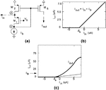
From my understanding and calculation M1 and M2 form a transimpedance amplifier with shunt feedback, which makes the input resistance at node x very low.

From Paper:
"Due to the shunt feedback provided
by transistor M2, the impedance at node X is very low
and, this way, the amount of current that flows through this node
does not modify the value of its voltage. Note that node X can
source large current variations at the input and the FVF translates
them into compressed voltage variations at output node"

-> What benefit do i get that the current through node x doesnt change the voltage because of the low impedance? What exactly does "node x can source large current variations" mean?


"Because of the feedback loop, the actual amplifier only has
to process the error signal, which is very small. That means that M2 must draw virtually the
entire input current Iin".

->can somebody pls explain this to me. Why is the error signal very small and why does M2 draw virtually the entire current?

Best regards
 

Attachments

  • 1487657-fig-3-source-hires.gif
    1487657-fig-3-source-hires.gif
    31.2 KB · Views: 140

If you disregard the input current for the moment, this circuit is just a cascoded current mirror - well, cascoded on the diode side. Current through M1 is fixed by Ib and it doesn't change. When you apply Iin, it can only go through M2. But if initially the gate of M2 is fixed, the application of the Iin will either reduce or increase Vgs of M1 momentarily. Then Ib will by the virtue of the feedback change the gate voltage of M2, so that it takes the extra Iin on top of the constant Ib. Since the gate voltage of M2 changes, so does the current out of M5.
Thus, the feedback tries to regulate the Vgs of M1 to be constant so that it can always pass the constant Ib. But since the gate of M1 is at a fixed potential so is its source, more or less. That is, you have some varying current into node X but the voltage of node X doesn't change a whole lot - this is a result of low impedance level at node X.
When you have a circuit with a current input, that input is designed to have low impedance. The output is taken from the drain of M5 and it is a relatively high impedance, acting as a current source. In this case the circuit is like a current controlled current source.
 
Last edited:
Thank you sutapanaki, i (hopefully) kind of understand what you described. But just to make sure i repeat it in my own words.

The feedback which causes the low input impedance is necessary to keep Vgs,1 constant. So if i apply a signal current Iin the extra current through node x wont change the source potential that much because of the low impedance. Since the gate of M1 is fixed Vgs,1 is approximatly constant.
That means that nearly the entire signal current has to flow through M2. This current sets the output signal, which is a voltage at the drain of M1 if you only consider M1 and M2. Thus the structure of M1 and M2 forms a transimpedance amplifier (current controlled voltage source). This voltage is also applied to the gate M5 and can be used to generate replica currents Of the Input current Iin so the whole structure including M5 is a current controlled current source.

In the case Vgs,1 is not approximatly constant there is an extra signal current thorugh M1, which means that the signal current thorugh M2 it less then Iin and therefore the current copying to the output it inaccurate. Hence this feedback is necessary to achieve accuracy in first place.

I have some more questions:

1) This strucure can achieve class AB behavior because there is no tail current source which limits the total current and the total current is only dependant on the signal applied to the input. Did i understand it right?

2) If the source potential of M1 is approximatly constant, why cant i assume a virtual ground here? Or does this virtual ground concept only apply to node potentials that are 100% fixed and not only approximatly fixed. I mean virtual ground is of course wrong because i would short M2 completly, but i just want to know why its wrong.

And by the way you are right, the output impedance which is at the drain of M1 is approx 1/gm2 and compared to input impedance which is 1/(gm1gm2*ro) pretty high. Interestingly the gain of the structure M1 and M2 is an impedance (therefore trancimpedance amp) and is equal to 1/gm2. I have difficulties to understand what it actually means. I mean in the case of a voltage-voltage amp its easy, but what does it mean if i have a gain which is equal to an impedance? What qualities can i "assume" from it concering the amplifier.? Maybe how "good" the amplifier converts a current to a voltage? So the higher the transimpedance the better my amplifier?

Sorry for this big text.

Big thanks
 
Last edited:

Yes, pretty much you got it right. The Vgs1 has to be kept constant, because it conducts constant current Ib. I wouldn't necessarily consider the gate of M2/drain of M1 as really an output signal, because the relation between the input current Iin and that voltage is non-linear, except for small signals, but I guess if you are comfortable with this notion, you can also think of it that way.
If you don't have the feedback, say you connect the gate of M2 to a fixed voltage, then that fixed voltage will be only good for a fixed current. If you have some extra current Iin, for example going into node X, then it can't go into M2 because of the fixed gate voltage. So the voltage of node X will start to go in such a direction as to decrease the Vgs of M1 because M2 still wants to have the same current as per its gate voltage and the circuit will try to obey KCL at node X. So, as the Vgs of M1 decreases, the drain current of M1 decreases and the current source Ib will now dominate at the drain of M1 by pulling it down until the voltage across the current course Ib drops to almost 0 in the case when that current source is realized with transistors. When you have the feedback you avoid all this. and the circuit adjusts the gate of M2 for the current Iin.

1) Well, there is no tail node to begin with. Apart from that you are mostly right. However, when Iin becomes too high, requiring the Vgs of M2 to become large, at some point M2 will go into linear region and the circuit will saturate.

2) Virtual ground is sort of a modelling concept and an approximation. And as any model it is good in some cases and doesn't in others. From the point of view that the impedance of node X is low, because of the feedback, then yes, you can consider it a virtual ground. It is similar virtual ground as at the inverting input of an OPAM in an inverting configuration, only that the in the opamp case you have much more loop gain and hence better virtual ground approximation. Virtual ground doesn't mean you short something to ground, in our case the M2. It simply means the voltage doesn't have significant ac component, ideally none.

1/gm2 is not really a high impedance, and it is same as the impedance of any diode connected transistor. I agree, though it is much higher than that at node X. In my previous comment I was talking about the impedance at the drain of M5, which is ro and thus much much higher compared to both 1/gm2 and 1/(gm1*gm2*ro).
Transimpedance amplifier simply means that your input is current and you output is a voltage.. It converts current into a voltage.
 
Yes, pretty much you got it right. The Vgs1 has to be kept constant, because it conducts constant current Ib. I wouldn't necessarily consider the gate of M2/drain of M1 as really an output signal, because the relation between the input current Iin and that voltage is non-linear, except for small signals, but I guess if you are comfortable with this notion, you can also think of it that way.
If you don't have the feedback, say you connect the gate of M2 to a fixed voltage, then that fixed voltage will be only good for a fixed current. If you have some extra current Iin, for example going into node X, then it can't go into M2 because of the fixed gate voltage. So the voltage of node X will start to go in such a direction as to decrease the Vgs of M1 because M2 still wants to have the same current as per its gate voltage and the circuit will try to obey KCL at node X. So, as the Vgs of M1 decreases, the drain current of M1 decreases and the current source Ib will now dominate at the drain of M1 by pulling it down until the voltage across the current course Ib drops to almost 0 in the case when that current source is realized with transistors. When you have the feedback you avoid all this. and the circuit adjusts the gate of M2 for the current Iin.
Thx for the reply,

So if i connect the gate of M2 to a fixed voltage i pretty much get a Dc current source, that draws a constant current. Therefore the signal current cant go that way because the current is fixed. But to fullfill kCL at x the current through M1 has to drop which corresponds to a lower VGS,1. If i assume a large input current variation then my Vgs,1 drops to almost 0 in this case?

And yeah because of the feedback a large current variation leads to an adjustment of the gate of M2, and the current gets copied to the output again. And about the output signal at gate of M2, i thought it that way because i did the small signal analysis, but you are absolutly right. In case of large signal the behavior is nonlinear. But what about the output current? I mean for large input signals everything becomes nonlinear or am i wrong?

Your explanation with virtual ground helped a lot. Actually i didnt think about it as an approximation. I think im messing up some thinks. I applied virtual ground for the half circuit concept if i calculate the small signal differential gain for a class A differential input stage. But grounding this node only works if i have perfect symmetrie. In this case here there is no symmetrie. But if i think about a voltage that doesnt change with time, isnt it ac ground?

Best regards
 
Last edited:

Copying current from Iin to the output is pretty much linear even for large signal currents, provided that M2 doesn't go in linear (triode) mode and M5 is also in saturation. It is similar to the linearity of a current mirror. You can think of it in the following way - Iin causes non-linear voltage at the gate of M2 because of the square root dependence of voltage on drain current. But then there is a square law dependence of the drain current of M5 on its Vgs and thus it compensated for the non-linearity of the Vgs when the drain current is of interest.

Yes, a voltage that doesn't change with time is a virtual ground but it is not a physical short to ground. In the case of differential pair we think of the tail node as ac ground because of symmetry but that node is not really physically connected to ground. It just wiggles very little and we can safely think of it as carrying no ac signal - again, for small signals. An to do the small signal analysis we have the half circuit and connect that point to ground but it is not a physical ground.
 
Status
Not open for further replies.

Similar threads

Part and Inventory Search

Welcome to EDABoard.com

Sponsor

Back
Top