Continue to Site

Welcome to EDAboard.com

Welcome to our site! EDAboard.com is an international Electronics Discussion Forum focused on EDA software, circuits, schematics, books, theory, papers, asic, pld, 8051, DSP, Network, RF, Analog Design, PCB, Service Manuals... and a whole lot more! To participate you need to register. Registration is free. Click here to register now.

filter cap parallel on feedback resistor for buck dc/dc question

kaunasLT

Newbie
Joined
Mar 13, 2024
Messages
3
Helped
0
Reputation
0
Reaction score
0
Trophy points
1
Activity points
42
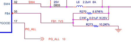
Looking at a TI application note they have placed the filter cap parallel to the resistor on the "high side" (see attached picture).

the capacitor would create a low impedance path for high frequency and almost have no voltage drop, wouldnt the high frequency noise then be sampled at the feedback node?

why not place the cap parallel across the lower side resitor such as when the high frequency of the switching noise see a low impedance to ground and the feedback node can measure low frequency DC to adjust the output?

Im asking this because I was playing around creating a DIY buck and have in my design placed the cap to give a low impedance to ground and would from there derive a transfer function i can further compensate digitally using PID.
 

Attachments

  • ti billed.png
    ti billed.png
    84.5 KB · Views: 53
In shunt with the feedback upper resistor, it gives you some "D"
for your PID, improving load-step response by "advance notice"
(and defeating somewhat, the input and routing capacitance of
the center, feedback node which causes feedback lag).

In shunt with the "lower" resistor a cap would add phase lag and
destabilize your loop (or increase the compensation needed, which
will hurt transient response).

Check out "Type 1", "Type 2", "Type 3" DC-DC compensation.
that makes sense. I suppose the cap should then be valued such as the impedance at the given vout voltage doesnt exceed the µC's voltage level.

If i may ask a follow up question, when deriving transfer function, should it be done with respect to VOUT or with respect to the feedback node (node between the resistor pair)
 
when deriving transfer function, should it be done with respect to VOUT or with respect to the feedback node
Feedback divider is part of feedback loop, its transfer function is V(fb)/V(out). You need to know all partial transfer functions (error amplifier, modulator, output stage) to design possible frequency compensation for the divider.
 
I agree with FvM.
Thus I recommended to contact the datasheet and/or additional informations provided by the IC manufacturer.
As EasyPeasy wrote: It is called "feed forward capacitor" ... and usually reduces ripply voltage and may reduce overshot.
Some kind like the "D" part of a PID loop.

Again: use the informations provided by the manaufacturer, they know best!

Klaus
 

LaTeX Commands Quick-Menu:

Similar threads

Part and Inventory Search

Welcome to EDABoard.com

Sponsor

Back
Top