ESD_student
Newbie level 1
Hello, I am a student studying ESD.
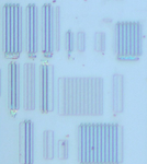
As far as i know, the main failures of ESD is a breakdown of gate oxide and the thermal breakdown of ESD protection or clamping circuit. So, I tried to take a picture of the breakdown point.
First, prepare a failed sample by ESD event. (i measure the leakage current)
Then, Dip it in a HF to erase the patterns. And take a pictures
But, there are some problems. 1. it is difficult to leave only the gate oxide because it is very thin.
2. I expected to see the junction damage of clamp but i did not see anything as shown in the below figure.
I would appreciate your advice. There is no one nearby to ask.
Thank you.

