Continue to Site

Welcome to EDAboard.com

Welcome to our site! EDAboard.com is an international Electronics Discussion Forum focused on EDA software, circuits, schematics, books, theory, papers, asic, pld, 8051, DSP, Network, RF, Analog Design, PCB, Service Manuals... and a whole lot more! To participate you need to register. Registration is free. Click here to register now.

Explanation for Via Filling Mask

Status
Not open for further replies.

soner86

Newbie level 5
Joined
Sep 8, 2008
Messages
9
Helped
1
Reputation
2
Reaction score
1
Trophy points
1,283
Activity points
1,329
Hi,

I encountered a blue mask applied to some specific vias of a PCB.
When I search for it, I found the following example:


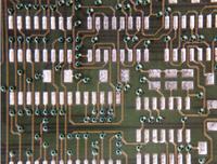
Do you know the aim?

"vacuum-tightness for the in-circuit test" is their explanation but I could not understand what the aim clearly is.

Here is the link: **broken link removed**

Thank you.
 

Could it be because, using a via as a test point has the possibility of damaging the via, breaking the barrel etc (there is a lot of pressure in a jest jig) so whatthis is doing is filling the via with a conductive masking.

This then allows the via to be treated as a testpoint.

IMO still not a good idea but if your stuck then your stuck and it may get you out of a hole.

As for the colour - its of no consequence.
 

Thanks Mattylad,
It is logical to strengthen a via which will be used as a test point. As far as I know, via plating method is also used for thermal purposes.
Actually the term, 'vacuum-tightness' had confused me. Thanks.
 

I don't think this is conductive paste.
I think in-circuit-tester uses vacuum holder, to hold PCB in place during testing.
 

Hi GUMY,
I think your suggestion is very good but holes of the vias do not seem to be filled. They may get rid of them at the end of the process. Thanks.
 

Status
Not open for further replies.

Part and Inventory Search

Welcome to EDABoard.com

Sponsor

Back
Top