Continue to Site

Welcome to EDAboard.com

Welcome to our site! EDAboard.com is an international Electronics Discussion Forum focused on EDA software, circuits, schematics, books, theory, papers, asic, pld, 8051, DSP, Network, RF, Analog Design, PCB, Service Manuals... and a whole lot more! To participate you need to register. Registration is free. Click here to register now.

[SOLVED] exciting a planar antenna

Status
Not open for further replies.

Vineeth m p

Junior Member level 1
Joined
Sep 22, 2012
Messages
19
Helped
0
Reputation
0
Reaction score
0
Trophy points
1,281
Activity points
1,418
Hi all,

I have a planar antenna structure modeled in HFSS.
The ground plane of the antenna structure lies in the same plane as that of the structure.
I dont know how to excite the structure. I don't know which excitation to be employed.
I got error when I tried wave port excitation and unexpected result for lumped port excitation.

Please help me.
 

Hi.
I want to help you but you should tell me more information about your design.
such as:
-what kind of feed do you use?
- what kind of antenna,you implement in hfss?
and for what's application?
 

Thank you for your interest...

The antenna which I am modelling is an ultra wide band(UWB) radio antenna.
The actual antenna is fed by PSF301 SMA connector.
Is that what you mean by the question of type of feed? uwb_antenna_1.pnguwb_antenna_2.jpguwb_antenna_3.jpg
 

hi.
ok. SMA is a coax feed.
you should use a coax for your design.
if you excited your design in side of antennna, you can use wave port or lumped port.
 

hi.
ok. SMA is a coax feed.
you should use a coax for your design.
if you excited your design in side of antennna, you can use wave port or lumped port.


What do you mean by excite in side of antenna? can you tell me with regards to the image i attached?
 

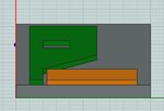
You can draw a rectangle in your X-Z plane. Assign wave port excitation to it with the integration line defined from ground to signal to make sure the correct mode is propagated. This should produce sufficiently accurate results.

Also, what is your substrate height and conductor thickness ? It looks like the conductor is a bit too thick...


You are true. The image which I added was one during the course of my design of the model. I reduced the thickness later, which now has a substrate thickness of 1mm and structure thickness of 0.02mm. I tried the wave port excitation as you said. But it results in some error, the report is copied below.

UWB_radio_antenna_solid (G:/ANTENNA THESIS/hfss/)
HFSSDesign1 (DrivenModal)

[error] Port refinement, process hf3d error: Port 1 is assigned to an internal face. Only allowed with lumped ports.. (1:52:05 PM May 04, 2013)
[error] hfsscomengine, process hf3d died unexpectedly. (1:52:05 PM May 04, 2013)
[error] Simulation completed with execution error on server: Local Machine. (1:52:05 PM May 04, 2013)
 

Sorry for the late reply. I was away over the weekend.

Take a look at this pdf [ https://www.scribd.com/doc/29255375/Port-Tutorial-CPW ]

When using waveport, there should not be any gap between the waveport rectangle and the radiation boundary airbox. So, fit your airbox X and Y right up to the edge of the substrate. Then you can leave the lambda/4 space for farfield calculations in the +- Z direction.

Draw a rectangle at the edge of the feed line (perpendicular to it) in the X-Z plane. The dimensions of this rectangle are explained in the pdf page 5. After that, draw the integration line correctly from the ground to the signal. The fields should look like the right figure of page 8 and not the left figure of page 8 in the pdf.
 
Status
Not open for further replies.

Part and Inventory Search

Welcome to EDABoard.com

Sponsor

Back
Top