Continue to Site

Welcome to EDAboard.com

Welcome to our site! EDAboard.com is an international Electronics Discussion Forum focused on EDA software, circuits, schematics, books, theory, papers, asic, pld, 8051, DSP, Network, RF, Analog Design, PCB, Service Manuals... and a whole lot more! To participate you need to register. Registration is free. Click here to register now.

[General] Esp32 drive electromagnetic contactor, controller and lcd getting noise and hang issue.

fawadbutt

Member level 3
Joined
Oct 29, 2010
Messages
61
Helped
4
Reputation
8
Reaction score
4
Trophy points
1,288
Location
Lahore, Pakistan, Pakistan
Activity points
1,754
Hi,
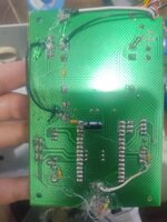
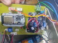
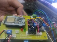
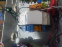
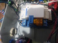
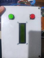
I try to drive electromagnetic contactor with esp32 controller and display some data on JHD 2x16 i2c (pcf8574)lcd. An d 2 button for some function.
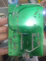
For this i schematic and made pcb.
But issue is that when electromagnetic contactor on or off . My circuit is disturb.moslty lcd start showing garbage and some time my esp32 controller hang.
For this try so many thing.
1- For connect Pcb board to i2c module use shielded wire.
2- add 0.1uf and 1 uf capacitor near to lcd and controller supply pins.
3- add 0.1 uf capacitor every input and output pins.
4- use 5v to 5v dc to dc isolated module for separate esp32 and lcd supply.
5- use copper pour hatch ground all over tha pcb and attach to external ground.
6- i use ferrid core ring in input and output wire.
But noise still come in board..
For electromagnetic contactor i drive 5 volt relay which drive 220 volt relay who operate contactor.
Kindly guide me what i doing wrong .
I think i need to design pcb again. For this give suggestions.
 

Attachments

  • IMG_20231029_180202.jpg
    IMG_20231029_180202.jpg
    1.3 MB · Views: 87
  • IMG_20231029_180157.jpg
    IMG_20231029_180157.jpg
    1.4 MB · Views: 69
  • IMG_20231029_180204.jpg
    IMG_20231029_180204.jpg
    1.3 MB · Views: 83
  • IMG_20231029_180211.jpg
    IMG_20231029_180211.jpg
    826.5 KB · Views: 60
  • IMG_20231029_180256.jpg
    IMG_20231029_180256.jpg
    4.3 MB · Views: 74
  • IMG_20231029_180251.jpg
    IMG_20231029_180251.jpg
    4.2 MB · Views: 70
  • IMG_20231029_180310.jpg
    IMG_20231029_180310.jpg
    1.5 MB · Views: 75
- isolate analog ground from power pulse current, avoid both conductive shared currents on Agnd (analog) and stray C coupled noise.
- use twisted pairs or shield TP or STP wires to help isolate offending power sources and sensitive inputs.
- use a wide range of low ESR caps for Vdd to gnd in a small area loop to broaden ESR bandwidth.
- use small 10:1 probe shorted loop to sniff stray EMI problem sources and orientations then contain it.
 
Hi, I'm really thankful for your guidance. I truly consider your advice, but unfortunately, I did not apply it to this PCB. I will keep it in mind for the next time. I just need tips for future circuit designing:

  1. Use FETs over optocouplers because they are more reliable for the long term and are suitable for fast switching. They also take up less space.
  2. Use a 2-layer PCB, with one side for the design and the other dedicated solely to ground.
  3. Incorporate ESD diodes for every input and output.
  4. Don't use isolation unless it's necessary.
  5. Include coupling capacitors on power supply and ADC lines.
  6. Avoid using mechanical relays, especially near the controller.
  7. Try to minimize the use of random long wires.
These are the things I've learned from this post. Thanks to all. If you have additional tips related to controller circuit design, I would be really glad to hear them
 
As important as your list, work out what paths the currents take. A good ground plane is always a good idea but also work out where other ground currents and supply currents flow. For example, if the physical path of a supply is: Source ----> load ----> CPU, and the path between source and load has high impedance or resistance, any drop along it, or interference fed in to it, will also appear at the CPU. Sometimes it is best to run an independent track to each load on the PCB, for example, from the supply input run one track to a relay and a different track to the CPU, that way there will be least interaction between them. Always use a driver transistor (bipolar or MOSFET) to drive heavy loads and remember that things like relays or LEDs do not need well regulated supply voltages so you can feed them from the source before the regulator. Using power tracks as wide as the board will allow will help minimize voltage drops.

Using mechanical relays isn't normally a problem but add a snubber diode across the relay coil as close to the relay pins as possible. Also, when inputs to a CPU are not speed critical, such as your switches, add a series resistor and a capacitor from the CPU side to ground to filter rapid changes such as interference spikes. Generally, if the inputs share the same ground as the switches or other control signals, there is no advantage to using opto isolation.

Brian.
 
You can learn more from studying the sinners (the failures) than the saints.
Rapid R&D fail and fix is better than slow conservative over-design.

"SpaceX will highlight the fact that it implements an iterative design approach and a fail-fast, learn-fast philosophy. Even if Starship explodes once again, the company will collect a wealth of data that will help it improve its chances of success in future launches." E.M.
 
Last edited:
As important as your list, work out what paths the currents take. A good ground plane is always a good idea but also work out where other ground currents and supply currents flow. For example, if the physical path of a supply is: Source ----> load ----> CPU, and the path between source and load has high impedance or resistance, any drop along it, or interference fed in to it, will also appear at the CPU. Sometimes it is best to run an independent track to each load on the PCB, for example, from the supply input run one track to a relay and a different track to the CPU, that way there will be least interaction between them. Always use a driver transistor (bipolar or MOSFET) to drive heavy loads and remember that things like relays or LEDs do not need well regulated supply voltages so you can feed them from the source before the regulator. Using power tracks as wide as the board will allow will help minimize voltage drops.

Using mechanical relays isn't normally a problem but add a snubber diode across the relay coil as close to the relay pins as possible. Also, when inputs to a CPU are not speed critical, such as your switches, add a series resistor and a capacitor from the CPU side to ground to filter rapid changes such as interference spikes. Generally, if the inputs share the same ground as the switches or other control signals, there is no advantage to using opto isolation.

Brian.
hi,
1- use power tracks wide for minimize voltage drops
2- use separate path route of power track and CPU track, from regulator or power source.
i learn these points from you, thank,
and yes i always use revers diode parallel on coil load , and use 100uf capacitor parallel on load. also use 0.1uf cap with ground on every digital and analog input,
can you guide me to to more secure I2C line which connected to multiple devices, i use 4.7K pullup.
 
I hope you mean 100uF parallel on the supply to the load, not the load itself!

What is not immediately obvious in any physical design is exactly where the currents flow. The schematic may show all the grounds and supplies connected to each other but in the real world there are obstacles to the current flow everywhere. Even in I2C you have to be careful where the voltage drops are. Consider that the SDA and SCL lines are pulled up to a supply by resistors so the voltage at the 'top' of the resistors must be clean RELATIVE to the ground of the I2C bus. It is the difference between ground and the signals that matter so if the pull-up supply or the ground have any voltage drops on them, it could appear as false clocks or data in the I2C stream. Also consider that although the resistance of the wires and copper traces may be very low, they have other properties, in particular inductance. As frequencies increase so does the reactance (effective resistance) of the paths. What may measure as a fraction of an Ohm on a DVM may be much higher at high frequency and the nature of spikes is they have a high frequency content.

Brian.
 

LaTeX Commands Quick-Menu:

Similar threads

Part and Inventory Search

Welcome to EDABoard.com

Sponsor

Back
Top