TokTok
Newbie level 2

- Joined
- Jan 9, 2014
- Messages
- 2
- Helped
- 0
- Reputation
- 0
- Reaction score
- 0
- Trophy points
- 1
- Activity points
- 21
Hi all,
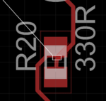
I'm designing a wireless relay card using eagle and I'm encountering clearance issues as indicated in the attached diagram.

I've been through the following sites to understand the clearance and its issues or errors:
**broken link removed**
http://en.wikibooks.org/wiki/Practical_Electronics/PCB_Layout
http://frontdoor.biz/HowToPCB/HowToPCB-Trace&Space.html
http://designinthetrenches.com/pcb-design/
https://www.edaboard.com/threads/240437/
I also read through and ran the DRC command (http://web.mit.edu/xavid/arch/i386_rhel4/help/42.htm) and its results indicated the clearance issues I have.
Below are the schematic and board files:
Schematic - http://sites.google.com/site/bgedsadownloads/EASYDAQ-XBEE.sch?attredirects=0&d=1
Board - http://sites.google.com/site/bgedsadownloads/EASYDAQ-XBEE.brd?attredirects=0&d=1
My grid settings are as below:
Size: - 1mm.
Multiple - 1
Alt: 0.025 inch
Display: on.
Style: lines.
Apologies if my questions sounds basic I'm still new to eagle, how can I get rid of this clearance problem.
Thanks.
I'm designing a wireless relay card using eagle and I'm encountering clearance issues as indicated in the attached diagram.

I've been through the following sites to understand the clearance and its issues or errors:
**broken link removed**
http://en.wikibooks.org/wiki/Practical_Electronics/PCB_Layout
http://frontdoor.biz/HowToPCB/HowToPCB-Trace&Space.html
http://designinthetrenches.com/pcb-design/
https://www.edaboard.com/threads/240437/
I also read through and ran the DRC command (http://web.mit.edu/xavid/arch/i386_rhel4/help/42.htm) and its results indicated the clearance issues I have.
Below are the schematic and board files:
Schematic - http://sites.google.com/site/bgedsadownloads/EASYDAQ-XBEE.sch?attredirects=0&d=1
Board - http://sites.google.com/site/bgedsadownloads/EASYDAQ-XBEE.brd?attredirects=0&d=1
My grid settings are as below:
Size: - 1mm.
Multiple - 1
Alt: 0.025 inch
Display: on.
Style: lines.
Apologies if my questions sounds basic I'm still new to eagle, how can I get rid of this clearance problem.
Thanks.


