Continue to Site

Welcome to EDAboard.com

Welcome to our site! EDAboard.com is an international Electronics Discussion Forum focused on EDA software, circuits, schematics, books, theory, papers, asic, pld, 8051, DSP, Network, RF, Analog Design, PCB, Service Manuals... and a whole lot more! To participate you need to register. Registration is free. Click here to register now.

driver circuit for my power circuit

Status
Not open for further replies.

gosrivats

Newbie level 5
Newbie level 5
Joined
Jan 21, 2012
Messages
10
Helped
0
Reputation
0
Reaction score
0
Trophy points
1,281
Location
Chennai, Tamil Nadu, India
Visit site
Activity points
1,347
i m currently working on this circuit.in the attachment...i have a problem with driver circuit i m using IR2110 as i have two high side and two low side....first of all i have doubt whether i can use high side and low side driver for this as the pulses are of different...can u guys help me out please
 

Attachments

  • Untitled1.jpg
    Untitled1.jpg
    44.9 KB · Views: 134
  • Untitled.jpg
    Untitled.jpg
    46.1 KB · Views: 141

This is an unusual circuit.
The waveforms are peculiar. It would help if it showed the proportions over a full cycle.

On the surface...
It looks as though the supply V is divided across the leftmost capacitors. The lower switches redirect current flow. Perhaps this action varies the load voltage? And preserves high efficiency?

I think I am getting my simulation to act right (although it's hard to be sure). I'm using analog switches, which permit current to flow in any direction.

The inductor introduces resonant action. As a result, large currents flow in various parts of the circuit. These currents are larger than those going through the load.

Further experimentation will be necessary, to figure out which type of switching device, N or P, is needed to act as switches, at which position.
 

thanks for the reply.@BradtheRad...its a bidirectional converter..the power flows in both the direction. left most capcitors are like the capacitors in half bridge network where whole voltage in left side is divided and charged in those capacitors. but i didnt get any large currents in the simulation. and that inductor didnt act as resonance too. wen i tried in hardware, i had a problem in high side mosfets( i took S1 and S2 as high side mosfets..is it right??) can i use IR2110 driver ic for high side driver mosfets as the switching pattern is unusual??
 

I am now getting step-down action at the right, after I disconnected CL.

My simulation has a DC supply at left.

Current flows toward the inductor through S1 or S2. This suggests the S2 symbol is backwards.

Current flows away from point 'b', through S3 or S4. This suggests the S3 symbol is backwards.

S1 and S2 can be regarded as high side, S3 and S4 as low side.
 

bradtherad....u r right thanks fot his...so can i use ir2110 for this??

Sorry I have no direct experience with this type of control IC, but I have an idea how it works.

In order to make it work, you would have to find a way to make it respond to either (a) rising/falling capacitor charge, or (b) to current through them.

Then there are two switches which need to be driven by the opposite polarity as the other two.

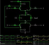
Here is a screenshot of my simulation. I believe this is proper operation. I installed switching transistors. They are oriented so the circuit works.

I find that the troublesome resonance has gone away, as well as the backward current flows.


Status
Not open for further replies.

Similar threads

Part and Inventory Search

Welcome to EDABoard.com

Sponsor

Back
Top