Continue to Site

Welcome to EDAboard.com

Welcome to our site! EDAboard.com is an international Electronics Discussion Forum focused on EDA software, circuits, schematics, books, theory, papers, asic, pld, 8051, DSP, Network, RF, Analog Design, PCB, Service Manuals... and a whole lot more! To participate you need to register. Registration is free. Click here to register now.

Doubts regarding on Example(C:\ADS2009\examples\MW_Ckt) amplifier Layout in ADS2009.

Status
Not open for further replies.
RealAEL Sir,
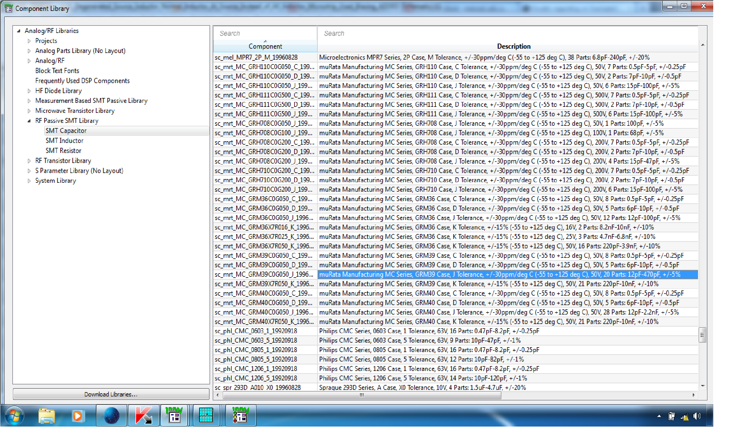
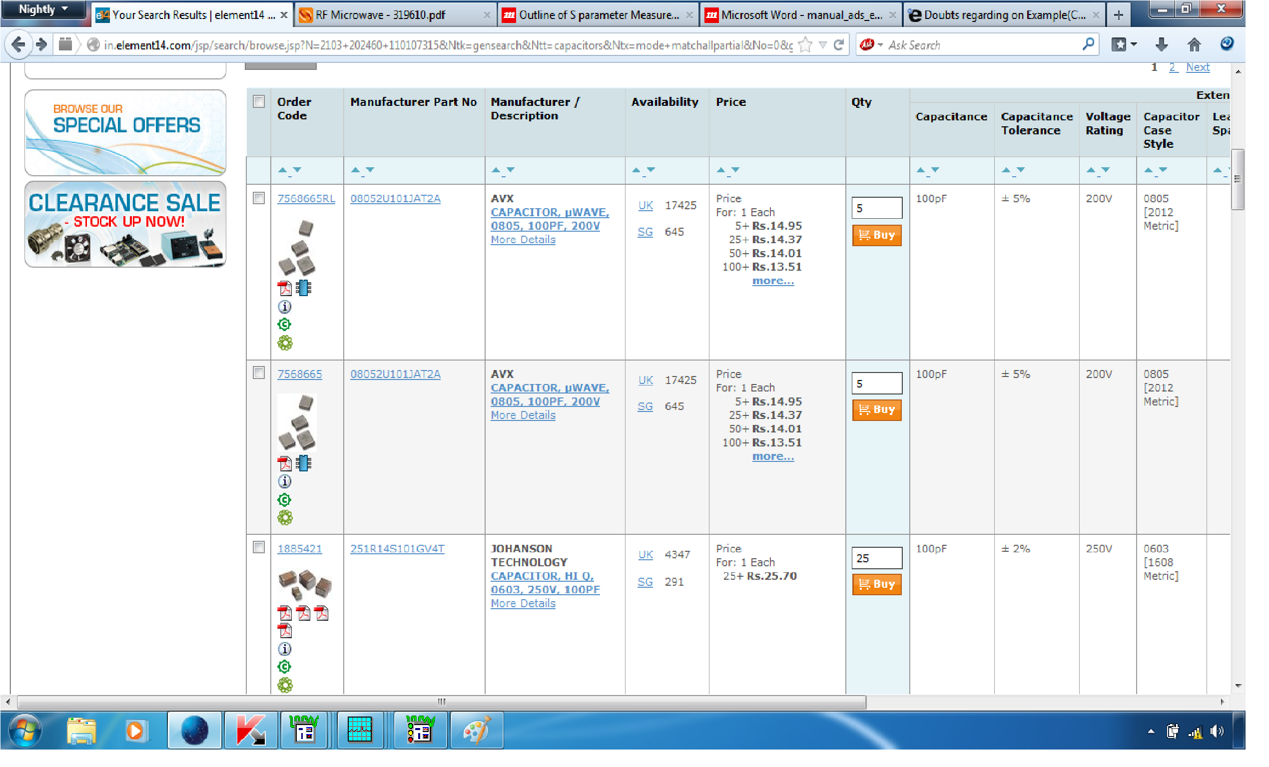
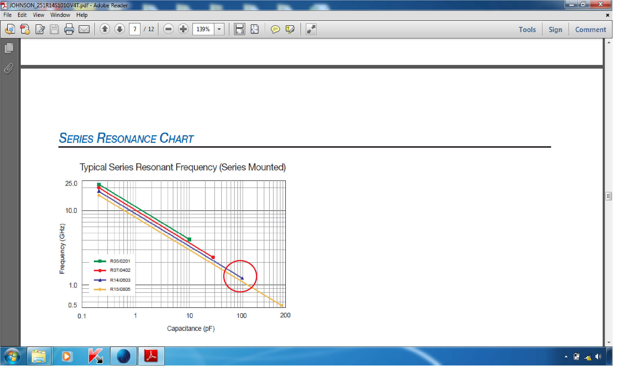
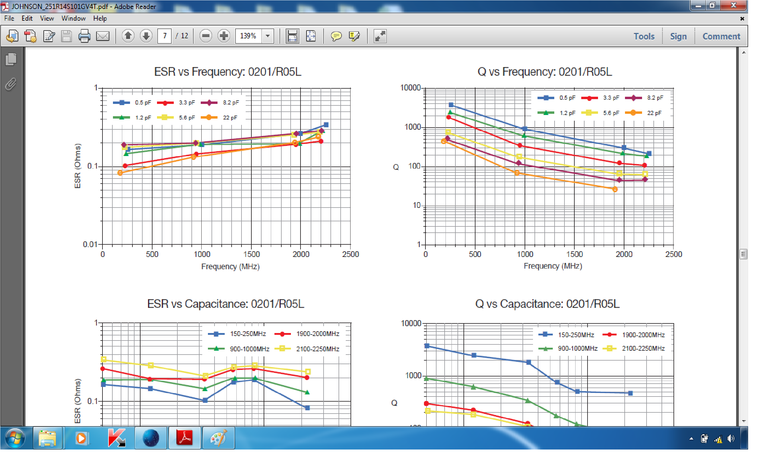
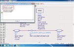
What is my difficulty is, my ADS 2009 SMT Library contains different companies capacitors (MURATA, AVX....) , resistors (AVX, BECKMAN......), inductors(ACT, Coilcraft.......) with different values with different part numbers. What I am choosing capacitors and resistors with different company and different part numbers from ADS 2009 SMT library. When I went and searched the commercial website (Like ELEMENT14),what ever present capacitors, inductors, resistors are available in the ADS library. Those same part numbers are not available in the outside market for capacitors, resistors and inductors and same companies components are available.

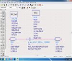
(1) Now I have created layout for LNA with the choosing the capacitors and resistors with different part numbers from SMT library. These capacitors and resistors with different part numbers are not available outside market. How we can get the market available components to our layout.

(2) Is there any possibility in ADS2009 to download those available market components and make utilize to our layout and latter fabrication. I have to get fabrication to my LNA layout

(3) Is there any possibility in ADS 2009, from my system always I can access the internet facility. Is there any possibility to access the market available SMT components directly to our schematic.

(4) Is there any possibility in ADS 2009. Can we attach the market available components to data item S1P SNP and make utilize it. If it is possible, how we can get the market available different part number components and latter to attach to data item S1P SNP and make utilize of those components.
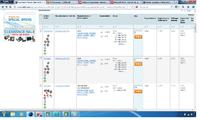


RealAEL Sir,
I went to the link as you have shown in the previous post, and asked request for them. One more thought came in my mind, go through the data sheet and take the market available part number. In the data sheet , we can find the Width , length, and offset of that component. Here In the ADS equivalent available library component we can take and substitute the market available component width, length and offset. Any how we are preparing the layout, for vacant space component, original fabrication we can get micro solder the market available vendor component. Is this way correct or not. If we follow this method , can we get the different results than expected results.
 

By altering the width, length and offset parameters all you would be changing is the layout representation of the pads that are used to attach the SMT device. You are not changing anything about the device itself. It would still be modelled using the built-in simulation data for the original part. For simulation purposes you need to use a model for the part you decide to use only.
 
RealAEL Sir,
I downloaded the 100 PF capacitors of AVX and JOHNSON companies. What I have noticed in the data sheet of those two companies graphs of series resonant frequency (SRF) vs Capacitor.

(1) In the first image(AVX_Company_100pf_Capacitor), they have shown SRF VS CAPACITOR graph, 0402, 0603,0805, and 1210 series. From the graph 0402 series, it says that 8.5 GHz to 2.5 GHz , which covers the 1 to 15 pf capacitor.Similarly 0603 series , it says that 8 GHz to 1.2 GHz , which covers 1 to 45 pf. 0805 series, it says that 7 GHz to 0.8 GHz, which covers 1 to 85 pf capacitors. 1210 series, it says that 6 GHz to 0.35 GHz , which covers 1 to 350 PF capacitors.
Our designing frequency is 2GHz LNA. Resonant frequency must be at the one frequency, in the graph why they have shown slope curve ( Example 0402 series 8.5 GHz to 2.5 GHz , which covers 1 to 15 pf capacitors). For example 0402 series , it starts from8.5GHz and stopped at 2.5 GHz, how we have to read the resonant frequency whether above 2.5 GHz or below 2.5 GHz( resonant frequency must be particular at one value?).

(2) What is the significance of series resonant frequency(SRF) in choosing the capacitors value for the layout creation. Our design is 2 GHz , which series capacitors is suitable(either 0402 or 0603 or 0805 or 1210) in the AVX company.

(3) I have also noticed the ESR graphs, what is the significance of the ESR in choosing the capacitor values.

(4) In the second image (Johnson_Company_100PF_Capacitor), in that graph also, you may notice R050201, R070402, R140603, and R150805. In this graph also , they have begun from one frequency and stopped at the other frequency. Here also , how we have to read the resonant frequency, from the stopped frequency below or above. Can you help me to understand.

I am attaching the images and relevant pdf files.


Attachments

  • AVX_08052U101JAT2A.pdf
    1.8 MB · Views: 48
  • JOHNSON_251R14S101GV4T.pdf
    684.5 KB · Views: 47

By altering the width, length and offset parameters all you would be changing is the layout representation of the pads that are used to attach the SMT device. You are not changing anything about the device itself. It would still be modelled using the built-in simulation data for the original part. For simulation purposes you need to use a model for the part you decide to use only.

RealAEL Sir,
As you said for simulation purposes , we can use the model. I went and selected palette > Lumped element > C_Model. But When I picked the C_Model from the lumped element and try to connect, it is not allowed to connect(it is showing red at the end of the connection). What I need to do for connection of C_Model and what we have to substitute for the select parameter(ex length =?, width =? , Cj= ? , Cjsw =? ) for 100PF capacitor.


RealAEL Sir,
I generated the layout for my work, later exported the layout generated file GERBER and DXF file. I have sent these files to the fabrication work.

(1)While exporting the GERBER FILE, it is creating the following files
bond.gbr
cond.gbr
cond2.gbr
hole.gbr
leads.gbr
packages.gbr
solder_mask.gbr
Now I saved these files in a one folder and sent it the fabrication work. Now he is asking , which are the above .gdr files related to the PCB(printed circuit board). My quesition is , which .gdr files are related to the PCB. Which .gdr files I have to tell for PCB related files to him.


(2) Even I exported the generated layout DXF file. He is saying that what ever DXF you sent to us, I am unable to open the DXF file. How we can export the DXF file to openable format in the PCB. Please help me.
I am attaching GERBER and DXF related file.
 

Attachments

  • BOTH_Gerber_and_DXF.rar
    12.2 KB · Views: 46

Gerber files always export as one file per layer from the layout with the name of each layer. You created the layout so you should know which layers represent what on the PCB. You can always use the command View > Layer View > By Name... to examine each layer in the layout and then the answer should be obvious.
 
RealAEL Sir,
As you said, I went to the command view > Layer View > By Name... and the noticed the following file

(1) cond
(2) cond2
(3)hole
(4)bond
(5)leads
(6)packages
(7)silkscreen
(8)solder mask

I viewed all the above files using the above layer view> By name.

When I went FILE> EXPORT>GERBER OR DXF and saved the GERBER or DXF.In the , Export GERBER file , I saved #47 posting files (Example bond.gbr,cond.gbr,cond2.gbr,hole.gbr.................) and sent to the PCB fabrication. PCB fabricator maker only, he is asking which files are related to the PCB.

(1) Sir, I am little confused, which files I have to tell him for PCB related files.I am new for this, can you tell me in detail sir. Even It is not allowed me to export the single GERBER file. When I went Command FILE > EXPORT > GERBER. It is saving a bunch of files as I discussed in the posting # 47 files.How I have to export the PCB related GERBER file and which are related to the PCB fabrication. Just I have created the layout and exported the GERBER and DXF file and sent it to the PCB fabrication. I don't know , which files are related to the PCB fabrication, Please can you make it clear sir.

(2) Even though I went FILE > EXPORT > DXF and exported the DXF file also.He is saying that" unable to open the format file sent by you,Normally all DXF files open without hitch" . How I have to export the DXF file, PCB fabricator can open DXF file.

Sir please help me.
 

All the files are coming from the layout so all the files have some data in them that may or may not be wanted for manufacruring the PCB. You have to look at each one and make the necessary decision. Use the View > Layer View > By Name... to look at each layer and decide what it is and if you need it. For example one layer may be the top metal, one may be the bottom metal (of double sided PCB), one may be drill holes for vias, etc. You are the only person who can make that determination and give that information to the manufacturer. If you do not need any layer then just do not give that gerber file to the manufacturer.

There are different versions/styles of DXF files that different software utilizes. If you have tried to communicate a file in this case and it is incompatible then that is all that can be done. There is no workaround to do anything different. Do not persue this format any further. (ADS 2009 is very old now so nothing can be changed with that)

- - - Updated - - -

Alternately, once you have determined the purpose of each layer and whether is is required for manufacturing or not you could then during the gerber export select the More Options... button, select the Layers tab in the pop-up UI and then only select the required layers for export rather than export all layers.
 
RealAEL Sir,
I have used VIA2 hole, drilling the substrate and make the connection from upper conductor to bottom conductor. I have read in one ADS LAYOUT TUTORIAL document , I am attaching that document. In that document following things have discussed for taking care while drilling holes

(1) Attached document page number 7 & 8 (page # 7, discussion points 6 and 7). They have told to choose the Edit Aperture , I have searched in the edit option, Edit Aperture option couldn't find. Where is that Edit Aperture option in ADS 2009.

(2) In the page # 6 & # 7, they have told to use metalization layer. To open the metalization layer we can use the command Momentum >substrate > create/modify > then hit the metalization layer, but there if we go the Momentum > Substrate > create / modify here we will find the layout layers. I couldn't find the metaliztion layer. Where is the metalization layer in momentum.

I request you to answer the above discussed points. RealAEL Sir,
I have used VIA2 hole, drilling the substrate and make the connection from upper conductor to bottom conductor. I have read in one ADS LAYOUT TUTORIAL document , I am attaching that document. In that document following things have discussed for taking care while drilling holes

(1) Attached document page number 7 & 8 (page # 7, discussion points 6 and 7). They have told to choose the Edit Aperture , I have searched in the edit option, Edit Aperture option couldn't find. Where is that Edit Aperture option in ADS 2009.

(2) In the page # 6 & # 7, they have told to use metalization layer. To open the metalization layer we can use the command Momentum >substrate > create/modify > then hit the metalization layer, but there if we go the Momentum > Substrate > create / modify here we will find the layout layers. I couldn't find the metaliztion layer. Where is the metalization layer in momentum.

I request you to answer the above discussed points.

- - - Updated - - -

RealAEL Sir
I am attaching the images
 

Attachments

  • ads_layout_tutorial_3033.pdf
    412.8 KB · Views: 458
  • EDIT_APERTURES.png
    EDIT_APERTURES.png
    587.7 KB · Views: 57
  • Metalization_LAYER.png
    Metalization_LAYER.png
    607.2 KB · Views: 68
  • Metalization_Layer_2.png
    Metalization_Layer_2.png
    336.7 KB · Views: 58

You will not find either of the items you request in ADS 2009. This tutorial appears to come from an older version of ADS (ADS 2006 or earlier). This set-up and the gerber exporter tool changed before ADS 2009. In the latest release (ADS 2013) it has changed again. The material you are using is obsolete.
 
RealAEL Sir,
While generating the layout from schematic, I am getting additional offset for the components like Capacitors, Resistors. How to remove this additional offset or avoid this. I have shown the offset in the red rectangular box in the figure name LAYOUT_Generated_For_Schematic that red rectangular box(offset) content. I want to avoid it or remove it. I have tried it for changing SMT_Pad PO value, it is not all changing. What I have to do for removing or avoiding the red rectangular content in the figure LAYOUT_Generated_For_Schematic.

While generating layout from schematic, even though we included SMT_Pad , it is showing the warning "No SMT_Pad item exists, using default Pad dimensions. To override default, place SMT_Pad item in Schematic". How to overcome this warning and how to avoid it, what I have done mistake.
I have attached the warning in the below figure Layout_Generate_From_Schematic_1
 

Attachments

  • SCHEMATIC.jpg
    SCHEMATIC.jpg
    520.2 KB · Views: 66
  • LAYOUT_Generated_For_Schematic.jpg
    LAYOUT_Generated_For_Schematic.jpg
    722.4 KB · Views: 62
  • Layout_Generation_From_Schematic_1.jpg
    Layout_Generation_From_Schematic_1.jpg
    472.2 KB · Views: 60
Last edited:

You need to edit the SMT capacitor parameters so that:
1. SMT_Pad is pointing to your PAD_0603 control and not set to the default Pad1. Then editing the SMT_Pad will make a difference to the layout
2. Use Offset parameter to slide the connecting pin to match the edge of the SMT_Pad layer that is under the end cap of the capacitor.

Should look similar to attached layout.

SMT.png
 
RealAEL Sir,
While layout generating, red mark is producing when there is connection between components and MLIN's. How to overcome this red mark between components and MLIN'S and how to avoid this red mark between Components and MLIN's. Below I have shown the SCHEMATIC and equivalent layout generated. In the generated layout , I have shown the produced red mark between Components and MLIN's.
 

Attachments

  • SCHEMATIC.jpg
    SCHEMATIC.jpg
    369.1 KB · Views: 61
  • LAYOUT.jpg
    LAYOUT.jpg
    430 KB · Views: 58

The color of the pin is not important, it is whatever you have set as you Highlight color in your Layout Display Preferences. It is usually cyan but can be any other color and canm easily be changed.

More important is the fact that the pin is showing as a diamond rather that a smaller rectangle. This is indicating that the pin at that location is not connected. Either the pin of the MLIN and the capacitor are not touching exactly and need to be moved to make the correct connection or the layer binding for the capacitor pins (on the ports layer) is not set correctly. If you select the capacitor and run the function Tools > Identify the two pins should show - "layer: ports, layer binding: *". If it just shows "layer: ports, layer binding: " or any different setting then the layer binding in the Layer Editor needs changing.
 
More important is the fact that the pin is showing as a diamond rather that a smaller rectangle. This is indicating that the pin at that location is not connected. If you select the capacitor and run the function Tools > Identify the two pins should show - "layer: ports, layer binding: *". If it just shows "layer: ports, layer binding: " or any different setting then the layer binding in the Layer Editor needs changing.
RealAEL Sir,
As you said and did it, I selected the capacitor selected the tools > identify and ran it. It is showing that the "layer:p
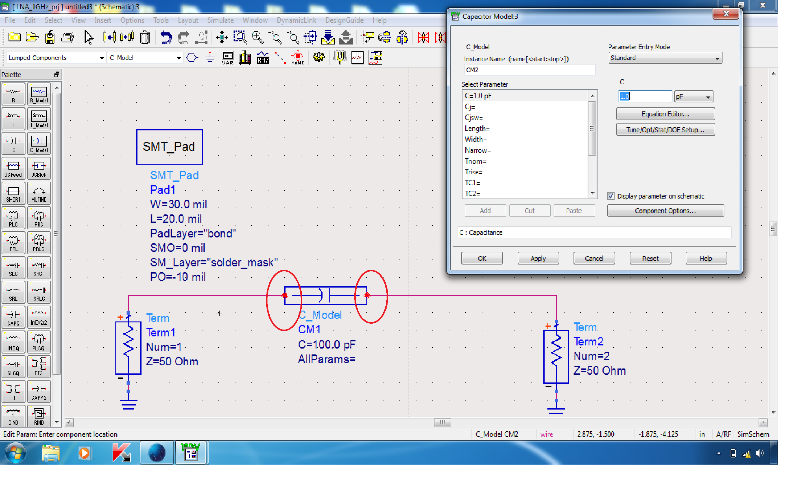
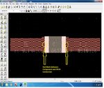
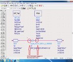
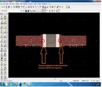
orts,layer binding", then what layer binding in the Layer Editor, we have to change , can you advice me. Even I run tools > identify, it is showing as like earlier red diamond symbol between connection of MLIN and Capacitor.
I have attached the both schematic and layout figures,and also attached the files of when ran the tools > identify.
 

Attachments

  • SCHEMATIC_1.jpg
    SCHEMATIC_1.jpg
    385 KB · Views: 56
  • Layout_View_1.jpg
    Layout_View_1.jpg
    391.2 KB · Views: 59
  • Identify_Run_Information.rar
    1.1 KB · Views: 43

As I posted previously if it just shows "layer: ports, layer binding: " then the layer binding for that layer needs changing in the Layout Layer Editor.
 
layer binding for that layer needs changing in the Layout Layer Editor.
RealAEL Sir,
I am sorry that I went to the layout layer editor, I am unable to find out the which layer is binding for that layer,can you diagrammatically explain it, please excuse me.
 

Attachments

  • Layout_Layer_Editor.jpg
    Layout_Layer_Editor.jpg
    388.6 KB · Views: 54

You need to scroll down the layer list until you find the layer(s) you need to modify and then set the binding on the second (Advanced) tab in the layer editor.
 
Status
Not open for further replies.

Part and Inventory Search

Welcome to EDABoard.com

Sponsor

Back
Top