Continue to Site

Welcome to EDAboard.com

Welcome to our site! EDAboard.com is an international Electronics Discussion Forum focused on EDA software, circuits, schematics, books, theory, papers, asic, pld, 8051, DSP, Network, RF, Analog Design, PCB, Service Manuals... and a whole lot more! To participate you need to register. Registration is free. Click here to register now.

Doubts regarding on Example(C:\ADS2009\examples\MW_Ckt) amplifier Layout in ADS2009.

Status
Not open for further replies.
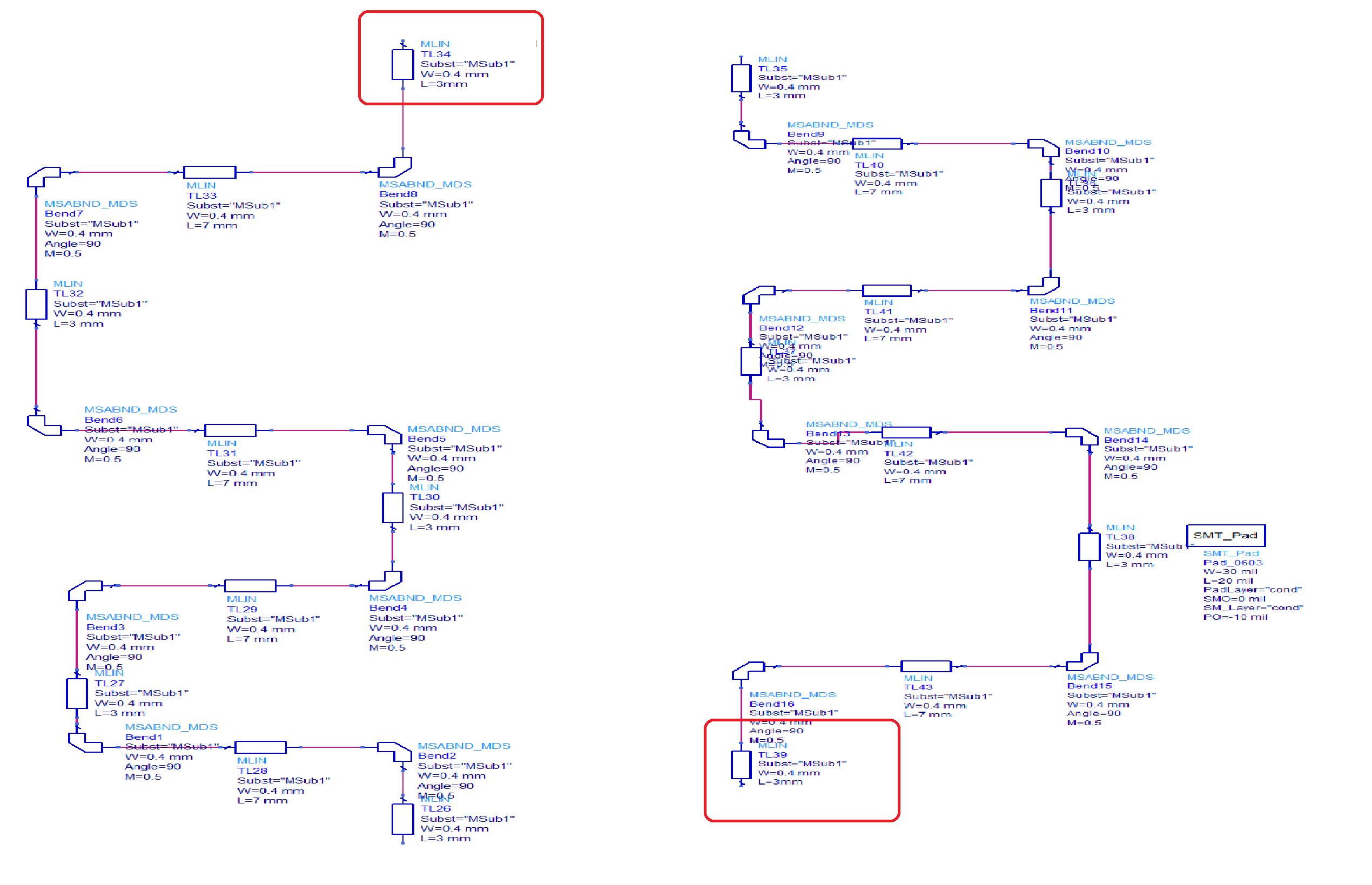
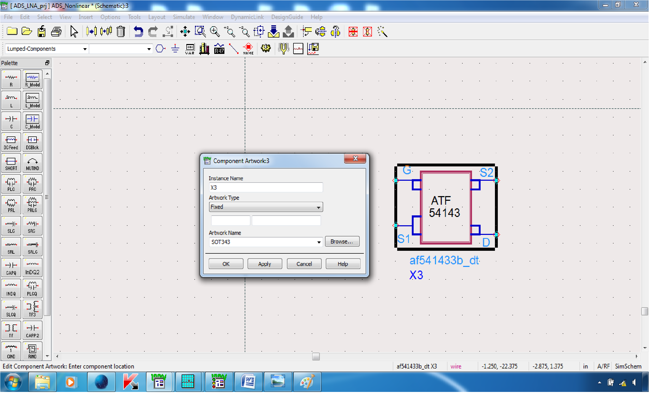
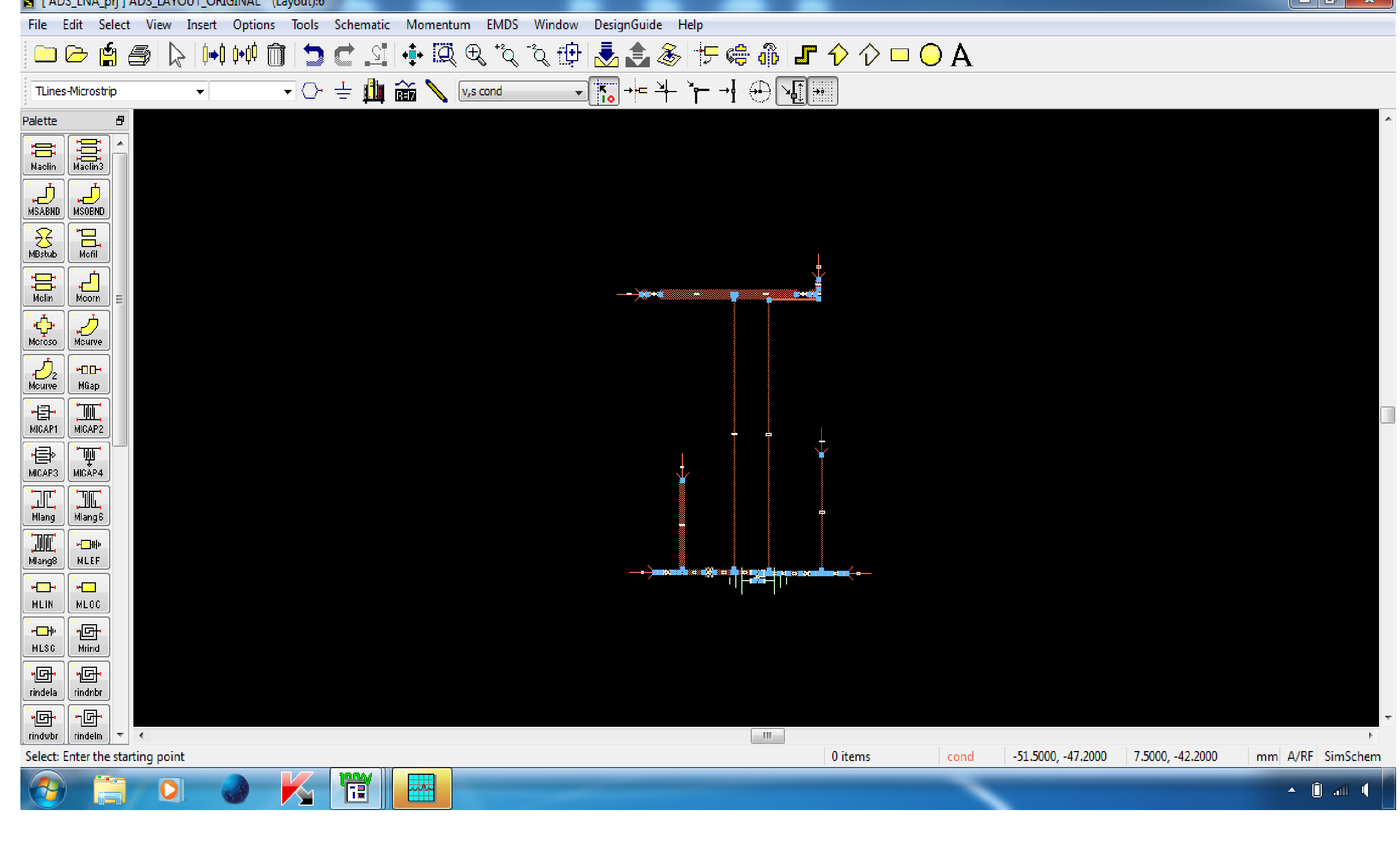
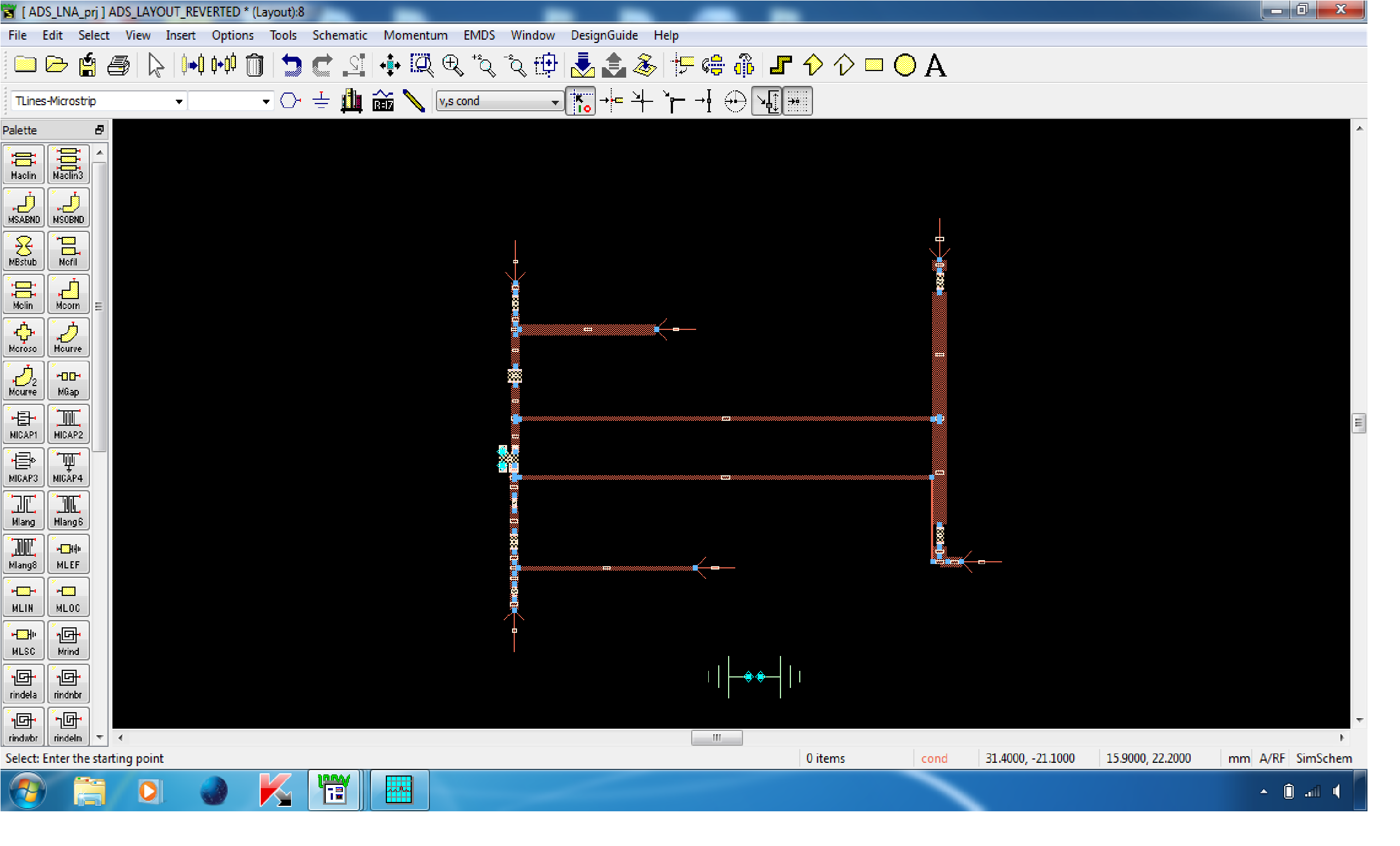
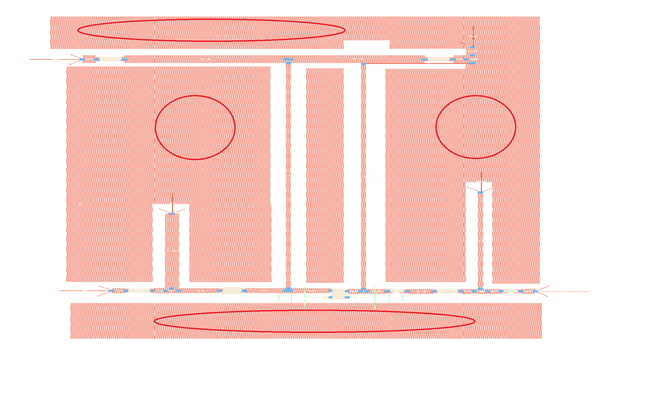
The error messages are about MLINs TL34 and TL39. Don't know about TL39 as it is not part of the schematic you provided but TL34 is there. For the L parameter of that MLIN you have entered 3mm for the width. Try 3 mm (with a space) and that one should work. It may be the same for TL39 but cannot tell.
 
RealAEL Sir,
When I added the MCORN and MSABND to the schematic and generated layout. Those letters Bend ,Tee and Corn are appearing in the layout, how to remove these appearing letters in the layout . Which option I need to choose the remove letters from the layout in the ADS. Below layout figure shows the appearance of the letters in the layout.


RealAEL Sir,
I have used MLIN 34 with L= 3mm and W= 0.4 mm, and have MLIN 39 with L= 3 mm and W = 0.4 mm. You told to try space 3mm means that I have to use W =3mm. I didn't get , what I have to use for space, is it a Width(W) or Length(L)?. I request you to see the posting of #22 problem sir, in that Bend, Tee and Corn letters are appearing , how to remove these letters in the layout.


- - - Updated - - -

RealAEL Sir,
I have used MLIN 34 with L= 3mm and W= 0.4 mm, and have MLIN 39 with L= 3 mm and W = 0.4 mm. You told to try space 3mm means that I have to use W =3mm. I didn't get , what I have to use for space, is it a Width(W) or Length(L)?. I request you to see the posting of #22 problem sir, in that Bend, Tee and Corn letters are appearing , how to remove these letters in the layout.


This is just annotation text so it does not change the design itself. However, some parts have smaller textthan this section so either you have changed the layout units part way through of changed the layout preferences. See this for some details:

Setting Design Environment Preferences

More details in the section about "Setting Component Text/Wire Label Options". Use the command Edit > Component > Component Text Attribute to change the annotation text for elements that are already placed in the layout.

Changing Component Text Attributes

- - - Updated - - -

Please read what I posted. I said not to use 3mm but to use 3 mm (with a space). If it is unclear that means 3<space>mm. It doesn't matter about spaces anywhere else but between the value and the multiplier it is important for ADS. You have done the same for the L parameter on both TL34 and TL39. Make sure that both have this space.
 
RealAEL Sir,
As you said, I followed, everything got correctly. You helped me each and every step of layout creation. Thank you very much for your patience, knowledgeable,priceless,timely help. Still one thing I am not getting correctly.


I shown in the schematic red ring left side TL62 , red ring right side TL69. I have generated the layout for this schematic, every time TL62 or TL69 moving left side or right side improperly. Either TL62 will move right side or left side or TL69 will move right or left side at once. I have shown in the layout, TL 62 moved left side improperly(it is shown in the red ring), it should be there at the yellow ring. Every time, when I generated layout from schematic, TL62 or TL 69 either move left or right side improperly.Sir What I have to do for correct positioning generation of TL62 and TL 69 without moving improperly left or right side.


Although you have not shown enough of the design to know the exact details you have created an impossible design that can never work. You need to be a lot more careful and have a better understanding in relative dimensions to get this to work.

1. The left meander overlaps other parts of the circuit. If everything snapped together as specified TL85 & TL56 will run over TL45 and create a short-circuit.
2. When you have a structure that connects in a complete loop, like the two narrow meander sections and the TL43/TL44 and the resistor between them and an equivalent section at the bottom I presume, you need to be precise in defining all the sizes of these parts. You need to calculate everything to fit exactly. ADS will not automatically resize parts to fit if they are wrong.

Just to demonstrate try deleting, temproarily, the schematic wire above TL56 and make it open circuit until you see what is happening. With that schematic wire removed regenerate the layout. Then you will see the overlap of the meanders. In this state you will also be able to deduce from the disconnect in layout what needs to be changed. Unless the "break" in the loop is adjusted to naturally fit back together the design will never connect correctly. The net vertical offsets each side of the structure and net horizontal offsets on the top and bottom of the structure need to match the other exactly.
 
RealAEL Sir,
I got it as you said, I followed it. Thank you very much sir. What must be the minimum separation distance between two DIFFERENT MLIN's to avoid the coupling losses, while creating layout we need to take care. What minimum distance is allowed between two DIFFERENT MLIN'S to avoid coupling losses.
 

You cannot avoid coupling between transmission lines. All you can do is to try to minimize any coupling effect and how you do that depends on the substrate material and the W/H ratio of the lines themselves. The usual compromise is to keep lines a couple of track widths apart at least but it really depends on the application and the space you have available. If there is any concern that is where you would simulate the citical parts of layout using EM and substitute that model for the transmission line based model.
 
RealAEL Sir,
It is working nicely,thank you very much sir. I designed amplifier using Avago ATF 54143 , but it's artwork of the transistor is not available. I right click on the ATF 54143 non linear device model , select the component> edit component network ,select the SOT343 (Artwork name). Is SOT343(artwork name) correct for the layout of the ATF 54143 transistor, how to adjust the OFFSET(pad offset-PO) of this transistor artwork . I simulated both linear without biasing and nonlinear with biasing. I have created layout for nonlinear with biasing ( there is no non linear device transistor model available in market, non linear device model is just electrical model). Can I go for this nonlinear( linear device model is available in the market) with biasing and created layout for the non linear device model with biasing for fabrication. Avago ATF 54143 it is not available in the ADS library, we can externally add it by using the data item S2P. But externally added data S2P, art work generation is not possible. I have shown below the image of artwork of ATF 54143.


The SOT package is being referenced as a fixed artwork. There is no option to modify the offest for the ports.

Why are you concerned about the layout for the linear device model. The layout should be exactly the same as the non-linear device model. So as long as the two schematic circuits are the same except for the model for the transistor then there should be the need to make only one layout. All you need to be sure is that the schematic symbol pins correspond to the equivalent layout pins.

It is possible, if the S2P data file symbols is configured in a 4 port schematic, to use exactly the same SOT fixed artwork package for that device also but really it is unnecessary as there should only be one layout anyway.
 
RealAEL Sir,
When ever I create the schematic and press layout > Generate / Update layout button for the generation of layout. First time it will come usual way ( Which is shown in the image ADS_LAYOUT_ORIGINAL), how we have shown in the schematic. For the same schematic second time, if we press the layout> Generate/Update layout,the layout what ever it is coming first time , it is reverted by 90 degree or 270 degree. Even though when we log out from the ADS and once again restart the ADS , once we go and open the layout schematic and press the layout > Generate / Update layout button, first what ever original layout, layout will be reverted either 90 degree or 270 degree or some other degree. Overall, once it is generated layout for first time,next time same layout is reverted by some angle. How to avoid the layout reversing 90 degree or 270 degree and retain first layout original appearance as it is first time created. I have shown the images the both original and reverted layout images.


When you do the Generate/Update layout make a note of the starting instance, location and angle entries. When you then Update the second time make sure the same values are those that are being used and you should get the same results. Different values may give different results. Otherwise clear the layout entirely before regenerating it.
 
RealAEL Sir
"Otherwise clear the layout entirely before regenerating it". I didn't understand sir, what I have to clear the layout entirely before regenerating it, can you tell it once. Will I have to make zero for X- co-ordinate, Y-coordinate and angle before regenerating. Can you make it clear.
 

RealAEL Sir,
Now it is working nicely, I deleted before generating layout. But one doubt, I have, if we have only upper conductor( we can generate it from the schematic) it is o.k.What is my difficulty is, generate the layout from the schematic and free hand drawing bottom conductor using polygon or rectangular. We have to retain that bottom conductor also. If we delete the layout(generated from the schematic) and free hand drawing bottom conductor. When we regenerate the layout, it layout only will come , once again we need to draw the bottom conductor using free hand. How we to retain both layout generated from schematic and the bottom conductor, which is free hand draw using polygon, when we regenerate the layout. I have shown in the below image, I need to retain both red ring shown portion and also layout generated from the schematic(without showing red ring portion). What we have to do.


If you do not want to delete everything then the solution is simple and obvious. Just do not use the delete all function. There are plenty of other selection options in the Select menu or using the select filter preferences to pick only the circuit based parts and not the polygon/rectangles before deleting and regenerating the layout.

The better approach though would be as I said previously to make a note of the starting instance, location and angle entries and make sure that those identical values are always used when Generating/Updating the layout from the schematic. Then the design will not move unexpectedly when regenerated.
 
RealAEL Sir,
As you said, I did. It is working nicely, thank you very much for your help.
 

RealAEL Sir,

(1)For creation of layout, I used spiral inductor MSIND from Tlines- Microstrip palette, connected in series with the source of the transistor. What is my doubt is, I have shown in the below image of the MSIND and MSSPLR_MDS. In MSIND, right side end is o.k, we can connect it anything, what ever we want. But in same MSIND left side end is passed above through the number of turns. While creating layout,will it not effect the inductance value or creation of layout, in that form is it O.k( left side it is passing on the number of turns,red ring shown part left side of MSIND). In MSSPLR_MDS , right side end we can connect it anything easily, what about at the center end (red co lour in the center), how we can connect this center end practical creation of layout.

(2)I have searched the entire palette list, spiral inductor is available in the Tlines-Microstrip palette list, is there anywhere available SPIRAL INDUCTOR in ADS 2009. While creating layout, if use spiral inductor in the schematic, will it automatically generate the spiral shape in the layout view?. For creation of layout of spiral inductor,is any other thing, do we need use like equivalent micro strip lines to connect it instead of spiral inductor. Which spiral inductor is better MSIND or MSSPLR_MDS.

(3) External inductor is nothing but palette lumped component inductor or some other inductor.Can you make it clear.


All printed spiral inductor will require some overpass or underpass structure to connect to the center of the spiral. These structures will certainly have an impact on the performance of the device. Some components, like the MSIND, have a layout that provides this structure and the model would also have some attempt to simulate these effects. Some, like the MSSPLR_MDS, do not have these structures so it is up to the user to create the overpass/underpass and define the model for this.

It has to be a choice that the designer makes as to which method is acceptable. EM simulation could also be used to create an appropriate simulation model if the built-in models are not as required.
 
RealAEL Sir,

(1) If use MSIND or MSSPLR_MDS for creation of layout.For creation of underpass or overpass, what we need to use for getting underpass and overpass.

(2) I used avago ATF 54143 transistor for my layout. It has four pin, two pins is for sources. Sources are internally connected each other. Suppose I want to use 1 nH at the source of the ATF 54143, then I use the 2 nH two inductors at the two sources , finally I will get 1 nH ( because two 2nH parallel inductor will give 1nH). Similarly MSIND if I want use N =2.0, Ri= 50.0 mil, w= 10.0 mil, s=10.0 mil. What values of MSIND( N= ?, Ri= ?, w=?,s=?) I have to connect at the two ends of the source,like that for getting 1 nH, I used 2 nH connected at the two ends of the source.


Status
Not open for further replies.

Part and Inventory Search

Welcome to EDABoard.com

Sponsor

Back
Top