pusparaga
Full Member level 4
Sir,
I have designed the two stage low noise amplifier using Advanced Design System 2009 at 1.7GHz. I have used the followings things to design the two stage LNA.
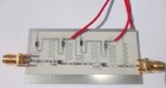
Transistor used is Avago ATF54143 transistor 3v,60mA
Rogers RT/duroid RO4003C is with following specifications
H(height of the substrate) =0.508mm
T(Thickness of copper cladding)=0.035mm
Er=3.55
TanD=0.0029
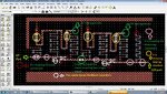
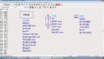
First I have designed the single stage LNA and later I have made it two stage by connecting coupling capacitor between two stages. First stage and second stage are the exact copy of each other separated by a coupling capacitor. I have not used Modelithics models of capacitor and resistors for my design of two stage LNA. I have used market available capacitor and resistors equivalent SRF and ESR matching capacitors and resistors to lumped equivalent values,have not used the inductors, instead of inductors, approximate MLIN's I used.
When I generated layout and simulated using ADS2009 , I have got the gain of 25dB, PCB fabricated and placed components measured the two stage LNA, I am totally getting 0dB gain.
What could be the reasons, why I got the measured gain 0dB for two stage LNA. But it was showing in the ADS2009 25dB at 1.7GHz.
What could be wrong,while designing two stage LNA,what could be the reasons behind the getting 0dB gain.
I have designed the two stage low noise amplifier using Advanced Design System 2009 at 1.7GHz. I have used the followings things to design the two stage LNA.
Transistor used is Avago ATF54143 transistor 3v,60mA
Rogers RT/duroid RO4003C is with following specifications
H(height of the substrate) =0.508mm
T(Thickness of copper cladding)=0.035mm
Er=3.55
TanD=0.0029
First I have designed the single stage LNA and later I have made it two stage by connecting coupling capacitor between two stages. First stage and second stage are the exact copy of each other separated by a coupling capacitor. I have not used Modelithics models of capacitor and resistors for my design of two stage LNA. I have used market available capacitor and resistors equivalent SRF and ESR matching capacitors and resistors to lumped equivalent values,have not used the inductors, instead of inductors, approximate MLIN's I used.
When I generated layout and simulated using ADS2009 , I have got the gain of 25dB, PCB fabricated and placed components measured the two stage LNA, I am totally getting 0dB gain.
What could be the reasons, why I got the measured gain 0dB for two stage LNA. But it was showing in the ADS2009 25dB at 1.7GHz.
What could be wrong,while designing two stage LNA,what could be the reasons behind the getting 0dB gain.