Continue to Site

Welcome to EDAboard.com

Welcome to our site! EDAboard.com is an international Electronics Discussion Forum focused on EDA software, circuits, schematics, books, theory, papers, asic, pld, 8051, DSP, Network, RF, Analog Design, PCB, Service Manuals... and a whole lot more! To participate you need to register. Registration is free. Click here to register now.

Doubt regarding over-current latch

sabu31

Full Member level 6
Full Member level 6
Joined
Jan 28, 2011
Messages
381
Helped
12
Reputation
24
Reaction score
12
Trophy points
1,298
Activity points
4,565
Dear All,
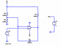
I am trying to simulate the overcurrent latch circuit (Application 5) given the datasheet of ACS712.

However, when I am simulating the system in LTSPICE, I am not getting the desired result. I am not able to understand the function of the Diode and Resistance R1. When I remove the diode, the circuit functions as required. What could be the issue?
 

Attachments

  • Current_Fault_Latch.pdf
    39.3 KB · Views: 28
  • Waveform_5.png
    Waveform_5.png
    8 KB · Views: 31

KlausST

Super Moderator
Staff member
Advanced Member level 7
Joined
Apr 17, 2014
Messages
23,242
Helped
4,738
Reputation
9,497
Reaction score
5,125
Trophy points
1,393
Activity points
153,951
Hi,

Unfortunately you didn't give the resistors the same names as in the datasheet. This can cause confusion.

Did you also use LMV7235?
Why didn´t you use the same resistor values as in the datasheet? 100k/100k makes no sense at all, because it means "trip at zero current". It´s like buying a fuse for 0mA.
(why using different values but complaining about different behaviour?)

I am not getting the desired result.
This is no error description.
What is your "desired result" and what do you see instead?

When I remove the diode, the circuit functions as required.
I doubt this. (For me: this makes no sense)
Please tell us what your required function is.

I am not able to understand the function of the Diode and Resistance R1
R1 (P_PU in datasheet) is the pull up resistor required for usual comparator outputs (open collector).
D1 is the "latching function".... as described in the datasheet: "This circuit latches an overcurrent fault and holds it until the 5 V rail is powered down."

Klaus
 

sabu31

Full Member level 6
Full Member level 6
Joined
Jan 28, 2011
Messages
381
Helped
12
Reputation
24
Reaction score
12
Trophy points
1,298
Activity points
4,565
I am sorry, I used MCP6021. However, even if I remove the diode it still works as a latch. Also I needed to disconnect the resistor connecting output to 5V rail.

The issue is due to LM7321 being an open collector?
 

KlausST

Super Moderator
Staff member
Advanced Member level 7
Joined
Apr 17, 2014
Messages
23,242
Helped
4,738
Reputation
9,497
Reaction score
5,125
Trophy points
1,393
Activity points
153,951

KlausST

Super Moderator
Staff member
Advanced Member level 7
Joined
Apr 17, 2014
Messages
23,242
Helped
4,738
Reputation
9,497
Reaction score
5,125
Trophy points
1,393
Activity points
153,951
Hi,

I really feel sorry that both share the same schematic symbol.

There are OPAMPs and comparators, and there is a good reason why they have different names.
They have different names, because they have different functions /operation modes.

OPAMP: (incomplete list)
* very low differential input voltage (say "zero"). Often needs some time to come out of saturation.
* output is analog, usualy never hitting the rail.

Comparator: (incomplete list)
* may have high differential input. Doesn´t suffer from saturation.
* output is digital, usually saturating hitting the one or the other rail (lower rail only, in case of OC output)

You may "mistreat" an OPAMP as comparator ... but often causes problems.
Sometimes you may "mistreat" a comparator as OPAMP ... but usually causes problems.
But I don´t understand "why" one would do so.

I would never come to the idea to use a round manhole cover as bicycle wheel .... just because it is round ;-)

BTW: you could do your own research on "difference between OPAMP and comparator", it gives me more than 1.5 million hits.

Klaus
 
Last edited:

    sabu31

    Points: 2
    Helpful Answer Positive Rating

danadakk

Advanced Member level 5
Joined
Mar 26, 2018
Messages
2,282
Helped
350
Reputation
718
Reaction score
527
Trophy points
113
Activity points
10,049
As you can see the diode changes the trip levels depending on what state
output is in. In effect it is a form of hysteresis. Hysteresis is symmetrical
about a trip point, this is asymmetrical due to diode.

Note it also is input amplitude sensitive, if I change the sine from 10V to 8V
pk-pk it wont switch, with output staying low. In effect it functions as a discriminator
of sorts.

My sim show's R1 does not effect anything, although I would think one
might observe a little higher 1 level out of OpAmp.

1676642986207.png


Regards, Dana.
 
Last edited:

LaTeX Commands Quick-Menu:

Similar threads

Part and Inventory Search

Welcome to EDABoard.com

Sponsor

Top