Continue to Site

Welcome to EDAboard.com

Welcome to our site! EDAboard.com is an international Electronics Discussion Forum focused on EDA software, circuits, schematics, books, theory, papers, asic, pld, 8051, DSP, Network, RF, Analog Design, PCB, Service Manuals... and a whole lot more! To participate you need to register. Registration is free. Click here to register now.

[SOLVED] Doubling a digital signal

Status
Not open for further replies.

ssulun

Newbie level 5
Joined
Jul 31, 2013
Messages
9
Helped
0
Reputation
0
Reaction score
0
Trophy points
1
Activity points
121
Hello everyone, I have a small problem to solve. Since I'm only a junior electronic engineering student, I don't have much practical knowledge. And I only have some experience with analog amplification, none with digital.

I have a digital signal coming from an Arduino microcontroller, a pulse train with 5 V amplitude, pulse width ranging from 5 to 20 ms, frequency ranging from 5 to 40 Hz. I want to double that signal's amplitude. My power source is a 12 V AC/DC adapter.

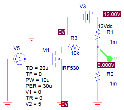
An experienced engineer has sent me the following design, and I've implemented it, but then the output's amplitude was ranging between 6.4 - 11.4 V. I thought about increasing the gain and get rid of the offset by using a capacitor, but then I realized it would be clipped off, since my supply voltage was 12 V.

irf.jpg

Then I thought about using a non-inverting op-amp, using two resistors with equal resistance, but somehow the amplitude was now reduced. It was even reduced in the negative terminal of the op-amp. (From my theoretical knowledge, I remember that ideally, both terminals should have equal voltage.)

Maybe there is a problem with the supply voltage, because in school, I could easily give plus and minus DC voltages, but now all I have is 12 V adapter. And since I've never used an adapter, now I'm having this huge confusion about what to do with the ground. Because I shouldn't feed the op-amp with +6/-6 V, since I need 10 V at the output. If I connect the positive and negative terminals of the adapter directly to the op amp, then what will the ground be? What to do with the ground terminal of the Arduino? (Because taking the input without any reference to Arduino's ground makes it noisy.)

In my trials, I've simply connected the adapter's negative terminal, and Arduino's ground together and took that as a ground. It might be a huge mistake, I don't know.

I also don't know if I'm using the right op-amp. In the workshop, I had a TL081CN, so I just used that. I don't know if it's not right to feed it with an adapter. Is there a specific type of op-amp that I should use? If yes, and if I don't have it, would it be simple enough to build my own amplifier with some transistors (I don't have much space on my PCB).

I hope you can help me out.

Thanks in advance.
 

OK, two solutions, depending on whether the Arduino ground (0V) is connected to the LED driver ground or not.

If the grounds ARE connected: remove the 8.2K resistor and it should work.
If they are NOT connected:

1. Take the output of the Arduino, through the 1K resistor to the anode of the LED side of an opto-coupler (6N139 for example) and ground the cathode side back to the Arduino.
2. Take the output emitter pin of the opto-coupler to the LED driver ground and connect the collector pin to the 10K resitor and LED driver input.

The second method isolates the two systems, using an IR LED and sensor inside the optocoupler to carry the pulse.
You should note that the schematic you have provided and both the methods I suggested are inverting circuits, a high input produces a low output and vice versa. If you want the polarity to be the same, use the opto-coupler but connect the collector pin to the supply voltage and put the 10K resistor and LED driver on its emitter pin.

All this assumes the LED driver is expecting a voltage to operate it and not a high current. If current is needed, it can still be done easily but extra components are needed, let me know.

Brian.
 
  • Like
Reactions: ssulun

    ssulun

    Points: 2
    Helpful Answer Positive Rating
Thanks for the quick reply. Yes, the grounds are connected, but the problem is, those grounds are also connected to the adapter's negative terminal. Even when I've removed the 8.2k resistor it didn't work, since when I check the Vcc with my oscilloscope, I'm seeing a pulse train with a base voltage of 3.68 V, and the maximum is 4.40 V. I'm guessing it is due to the usage of adapter (12.5 V AC/DC) to both power up the Arduino and to feed the transistor.
 

There will be a small 'lifting' of the logic low level because of the current through the 8.2K resistor but removing it should make the signal follow normal logic levels. The MOSFET should not conduct into it's gate pin from it's drain pin and it shouldn't draw any current into it's gate from the Arduino. The voltage at the gate (without the 8.2K) should be normal logic levels. That's 0V when low and (I think) 5V when high. When you say 'Pulse train', where exactly are you measuring? The current drawn from the adapter is very small (about 1mA) so the voltage it produces should be fairly constant at around 12.5V.

Brian.
 
  • Like
Reactions: ssulun

    ssulun

    Points: 2
    Helpful Answer Positive Rating
You're right, it is 5V when it's high.

The schematic that has been sent to me has also another 10V, feeding the gate. When I get rid of that 8.2kohms, I shouldn't feed the gate anymore, right? I didn't understand its purpose anyway. Again, I haven't had a course on digital design, but I think 5V at the gate would be enough to turn the MOSFET on.

I measure the pulse train between the Arduino's ground and one of its digital pins. I should note that the Arduino's ground is the same as the adapter's negative terminal. More experienced colleagues defined the pulse train as "pulse width modulation".

So when the voltage feeding the drain is 12.5, I should get a drain current around 250uA so that my output would be 10V, right? I wanted to apply my very basic formulas for hand calculations, but couldn't find the parameters like lambda, an exact threshold voltage, uCox, W/L etc. on the datasheet, what a shame:) Maybe there are some other parameters and formulas that I should use for transistors this large, I have so much to learn...
 

Don't worry too much about those parameters, what is important here is that the MOSFET gets turned on and off like a switch. The gate draws virtually no current so regardless of whether the Arduino output is 0V or 5V, no current should flow into it. Being an enhancement mode MOSFET, when the Arduino produces 0V at it's output, the MOSFET should be non-conducting and with 5V, hopefully the drain sinks current and pulls it's voltage close to zero (like a closed switch to ground). Where there may be problems is that the IRF530 gate voltage to be fully conducting may need to be more than 5V. The actual voltage needed is to some degree governed by the drain current and as you are asking for doubling 'signal' and the drain resistor is 10K, I assume the LED driver signal is a voltage doesn't need much current to drive it. The maximum current should be around 1.25mA (12.5V/10K) so you could use a much smaller MOSFET or better still, a small bipolar transistor. A bipolar device will only need around 0.65V so it is well within the Arduino's capability to drive it.

Brian.
 
  • Like
Reactions: ssulun

    ssulun

    Points: 2
    Helpful Answer Positive Rating
Thank you so much, now it seems to be working but I've just received an update about the project. The thing is the pulses coming from the Arduino were at 32kHz. So using this circuit, the output is not exactly a pulse. There is some slew, like when the pulse width is 10us, the rise time is 5us. Is IRF530 not suitable for this frequency range, or do you think there is some capacitance somewhere?
 

There are indeed capacitances and the IRF530 probably isn't the best device to use. The biggest problem you will see is that the Arduino output has to rise to about 3V before the IRF530 starts to conduct at all so the start of the natural rise in the front edge of the signal is being wasted. Those rise times are still short in comparison with 32KHz period though (~31uS)

Before going further, how much current is passing through the LED driver connections? Is the driver connection an off/on control input to a driver circuit or is all the LED current passing through the driver connections? the reason I ask is that if the driver input is simply to be driven high or low with a voltage, a bipolar transistor will be far more suitable and faster acting. Do you have a specification for the LED driver you could show us.

Brian.
 
  • Like
Reactions: ssulun

    ssulun

    Points: 2
    Helpful Answer Positive Rating
I've finally observed a decent square wave at the output, but now I see that you're right about that concern. I see former colleagues has noted "1V=100mA" on the LED driver, but after that circuit, even though it supplies around 12V, the current which arrives to the LED driver is around 6mA. I have never worked with an LED driver or a digital switch before, so is this because the output resistance of the MOSFET is low so that we've created an alternative pathway for the current that we need?

So now which BJT would you recommend? And do you think the design with BJT will be as simple as the design with the MOSFET, or should I do some reading on "BJT as a switch"?

Thanks
 

It's difficult to give an accurate answer without more information on the LED driver but from what you describe, it has a voltage input so presumably it has a low current demand into the input pin. First look at the differences between a bipolar and MOSFET driver:

MOSFET:
1. needs very little drive current at it's gate so the Arduino doesn't have to 'push' hard to turn it on.
2. needs ~3V at it's gate to bring it into conduction (not good in this application)
3. when conducting, presents a low resistance to ground across the LED driver input (good).

Bipolar Transistor
1. needs a small drive current into it's base pin but in this application the amount should easily be within the capabilites of the Arduino.
2. needs ~0.6V at it's base to start conducting and ~0.75V will take it to full conduction.
3. when conducting, pulls the LED driver input down to ~0.2V (not as good as MOSFET but almost certainly adequate)

As the current is low, I would suggest you try a PN2222 or equivalent as the transistor. It will be physically smaller than an IRF530 but should still run almost cold. The schematic remains the same, just change source to emitter, drain to collector and gate to base.

Brian.
 
  • Like
Reactions: ssulun

    ssulun

    Points: 2
    Helpful Answer Positive Rating
I've found out that there was a problem with the grounding, so now it works fine, thank you so much.

But now I have another thing in my mind. I've heard that the Arduino's that we are using aren't produced anymore, they've switched to producing 3.5V ones, instead of 5V.

I wonder if IRF530 would still work with that voltage. I've checked its datasheet, and for gate threshold voltage it says min=2V max=4V. Why is this variance, because of heat or something? Would it be risky to operate with 3.5V then?
 

I haven't got datasheets here at the moment to check the IRF530 specs but the gate threshold probably isn't a tightly controlled parameter in that kind of MOSFET. It's really intended for switching applications where the threshold would normally be well exceeded as part of the design to make sure it was fully conducting or cut off completely.

I would be cautious about using 3.5V, it may work, it may not but in any case there is no safety margin. A bipolar transistor only needs about 0.6V so it might be a better solution to change to one. Everything else stays the same.

Brian.
 
  • Like
Reactions: ssulun

    ssulun

    Points: 2
    Helpful Answer Positive Rating
Thank you so much Brian.

Sorry about asking too many new questions, but when you're an intern people keep coming with brand new requests.

Now we want the output to be adjustable. We thought about using a voltage divider circuit for Vdd. That way we can change one of the resistors whenever we want to adjust the voltage. Just as an example, I've simulated the following design on OrCAD:

8808868000_1378922969.png


The transient analysis for the marked node gives a square wave between 6V and 5.99999999V so it should be good. But when I implement it on the breadboard, I see zero. Where do you think the problem is? The program is a students' edition by the way. If this approach is not good, what else can we do?

Thanks in advance
 

Not a good way to do it!

You are seeing zero volts because the resistor values are far too high and even if the MOSFET is turned off, the leakage through it, your test meter and the load are causing all the voltage to drop across R1. Using Ohms law, all those extra current paths are in parallel to R2 so it has a low value and hence the large drop in the potential divider.

The answer to the problem depends on how much current flows into the load. Don't think of the potential divider as being just two resistors, think of it as having the resistance of the circuit it's connected to in parallel with them. If you ignore the load, it will work and that's what your analysis showed but as soon as you connect anything to it, the voltages will be completely wrong. A further complication with the values you chose is that the capacitance of the MOSFET and load is also in parallel with R2 so when the FET is off, the voltage will try to rise slowly to charge the capacitance but when it turns on, it discharges the capacitance very fast. You can simulate this by adding a capacitance (say 1nF) across R2 and seeing what happens to the waveform.

You can fix the problem by dropping the resistor values but depending on current into the load, they may have to be quite small, maybe only a few Ohms so the current drawn through them may be significant and the circuit will be very inefficient. If the load current is small, you could do it by shorting R3 and dropping R1 to a lower value, say 1K Ohm then making a potential divider from R2 and a new resistor in series with it. In other words, let the MOSFET switch the full 12V across R1 then tap the voltage you want from a potential divider across the MOSFET.

Brian.
 
  • Like
Reactions: ssulun

    ssulun

    Points: 2
    Helpful Answer Positive Rating
Thanks!

I have tried lowering the resistor values, but then resistors lower than 50 ohms got very hot, higher than 500 ohms gave me jittering, and the ones between gave me pulses with a significant rise time.

The second method you proposed was a life saver. The output has proper pulses. They also asked me to make it non-inverting so I've added an extra transistor. Also, replacing the drain resistor with a 1k instead of 10k gave me a much lower rise time, I hope the trade-off doesn't give me any bad outcomes (lower resistor lifespan maybe?). I'm putting the final version of the design. I will wait for your and my colleague's approval before marking the topic as "solved". I hope it will be helpful to the ones that face this problem in the future.

non inverting.png

Thanks again.
 

That will work OK.

Something you should note though: The MOSFETs you are using are rated at 100V and 14 Amps but they are only working at 12V and 0.012 Amps so you could use very much smaller types with equal results. There is nothing wrong with using bigger devices than necessary but it generally takes up more space and costs more.

When you dropped the drain resistor and found it gave faster rise time, it confirmed what I said about the capacitance of the load. Try running your simulation on the original circuit again but add a capacitor across the MOSFET drain and source pins. It will be educational for you to see what it does and how it relates to the value of the capacitor and the drain resistor.

Brian.
 
  • Like
Reactions: ssulun

    ssulun

    Points: 2
    Helpful Answer Positive Rating
Status
Not open for further replies.

Part and Inventory Search

Welcome to EDABoard.com

Sponsor

Back
Top