Continue to Site

Welcome to EDAboard.com

Welcome to our site! EDAboard.com is an international Electronics Discussion Forum focused on EDA software, circuits, schematics, books, theory, papers, asic, pld, 8051, DSP, Network, RF, Analog Design, PCB, Service Manuals... and a whole lot more! To participate you need to register. Registration is free. Click here to register now.

Does diode connected NMOS automatically put it in Weak inversion mode?

Status
Not open for further replies.

sys_eng

Full Member level 4
Joined
Aug 3, 2016
Messages
193
Helped
0
Reputation
2
Reaction score
1
Trophy points
18
Activity points
1,489
What's the advantage of weak inversion?

Diode connected NMOS transistor normally used to set certain Bias voltage.
 

No, it only ensures that you will be at the border between
linear and saturation. The inversion "strength" depends on
the current being thrown at it.

There's not much "advantage" to weak inversion, it is just
where you end up when trying to do low power analog.
Or operate at low voltages (for reasons of chasing low
power, usually).

For FETs that are not tied D-G, some DC attributes
improve at lower Vgs (like Rout / gDS) and some get
worse (like gm) when you operate lower than VT0.
And things like AC bandwidth suffer quite a bit.
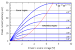

Well, isn't it VGS controls the current being thrown at it?
Because Gate and Drain tied then VGS is fixed therefore the current is already known.

look at the transistor curve, the different levels of current is controlled by VGS-Vth.

but diode connected transistor already has its VGS fixed so current cannot be varied.

500px-IvsV_mosfet.png
 

No, you are quite wrong. Tying gate to drain does not
apply any signal. That's a third connection. One which
up until now you have not described, but seem to have
some peculiar belief about.

Diode connected FETs as references, which is what
you did mention, are fed by current bias in normal
MOS analog design.
 

look at the transistor curve, the different levels of current is controlled by VGS-Vth. View attachment 140825

Yes, look at your diagram: the red curve means Vds=Vgs. Each point of intersection with the blue Ids-vs-Vds curves - actually any point on the red curve is a valid operation point for a "diode-connected" MOSFET (Vds=Vgs). The actual operation point is selected by the current injected into its drain.
 

Status
Not open for further replies.

Similar threads

Part and Inventory Search

Welcome to EDABoard.com

Sponsor

Back
Top