Continue to Site

Welcome to EDAboard.com

Welcome to our site! EDAboard.com is an international Electronics Discussion Forum focused on EDA software, circuits, schematics, books, theory, papers, asic, pld, 8051, DSP, Network, RF, Analog Design, PCB, Service Manuals... and a whole lot more! To participate you need to register. Registration is free. Click here to register now.

Distortions in SPWM inverter?

Status
Not open for further replies.

Artlav

Full Member level 2
Joined
Nov 26, 2010
Messages
144
Helped
2
Reputation
4
Reaction score
2
Trophy points
1,298
Activity points
2,723
Greetings.
Trying to make a sine wave inverter.
Sinusoidal PWM, an attiny85 driving an H-bridge with two IR2110 at 31KHz (two pins, one for \, other for /), filtered by two-pole LC filter (1.2mH+1µF, 4.7mH+0.47µF).

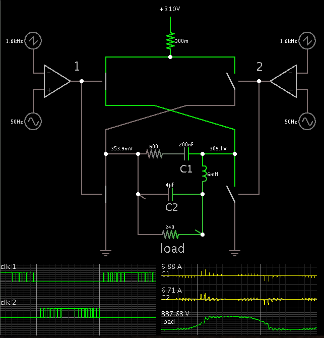
Schematic: http://orbides.1gb.ru/img/inv.png

Problem is, the output wave is distorted in a peculiar fashion:
http://i.imgur.com/nmGk9QS.jpg
(or http://orbides.1gb.ru/img/sine_bad.png )

The distortions do not depend on the way i generate SPWM, on frequency of either PWM or the generated AC, on filter or load.
Less or more samples in sine table makes the shape more or less fuzzy, but does not alter it's nature.

What could be causing such distortions?

Attiny code, variant one (both variants produce exactly the same waveform):
Code:
//#########################################################################//   
#define F_CPU 8000000UL
//#########################################################################//   
#include <avr/io.h>
#include <avr/interrupt.h>
#include <avr/power.h>
#include <math.h>
//#########################################################################//   
#define set_bit(port,bit) port|=(1<<bit)
#define clear_bit(port,bit) port&=~(1<<bit)
#define byte unsigned char
//#########################################################################// 
#define freq 50UL
#define table_count 100UL
#define prescaler 4UL
#define tim_delay F_CPU/(prescaler*freq*table_count*2UL)
#define PI 3.141592
//#########################################################################// 
byte sinetable[table_count];
volatile int cnt=0;
volatile byte side=0;
//#########################################################################// 
ISR(TIMER1_COMPA_vect)
{
 byte x;

 cnt++;
 if(cnt>=table_count){
  //One half-wave, then the other
  side=1-side;
  if(side==0){clear_bit(TCCR0A,COM0A1);set_bit(TCCR0A,COM0B1);}
  if(side==1){clear_bit(TCCR0A,COM0B1);set_bit(TCCR0A,COM0A1);}
  cnt=0;
 
  //Deglitch start of the half-wave
  TCNT0=0;
 }
 x=sinetable[cnt];
 OCR0A=x;
 OCR0B=x;
}
//#########################################################################//   
int main(void)
{
 clock_prescale_set(0);

 //PB0 and PB1 are \ and / of H-bridge
 DDRB=0x03;
 PORTB=0x00;

 //It takes a quarter of a second to fill in the x100 sinetable on board.
 //I don't care, if you do - use a precomputed table.
 for(int i=0;i<table_count;i++){
  sinetable[i]=floor(255.0*sin(((float)i/(float)table_count)*PI));
 }

 //31.25KHz SPWM
 TCCR0A=(1<<WGM00)|(1<<WGM01);
 TCCR0B=(1<<CS00);

 // /4 prescaler, frequency generation update timer
 TCCR1=(1<<CTC1)|(1<<CS11)|(1<<CS10);
 GTCCR=(1<<PSR1);
 OCR1C=tim_delay;
 OCR1A=tim_delay;
 TIMSK=(1<<OCIE1A);

 set_bit(TCCR0A,COM0A1);
 sei();

 while(1){}
}
//#########################################################################//

Variant two:
Code:
//#########################################################################//   
#define F_CPU 8000000UL
//#########################################################################//   
#include <avr/io.h>
#include <avr/pgmspace.h>
#include <util/delay.h> 
#include <avr/power.h>
//#########################################################################//   
#define set_bit(port,bit) port|=(1<<bit)
#define clear_bit(port,bit) port&=~(1<<bit)
#define byte unsigned char
//#########################################################################// 
#define table_count 100
#define freq 50
#define one_delay 1000000/(freq*table_count*2)

byte PROGMEM sinetable[]=
{
 0, 8, 16, 24, 31, 39, 47, 55, 62, 70, 77, 85, 92, 99, 106, 113, 120, 127,
 134, 141, 147, 153, 159, 165, 171, 177, 182, 188, 193, 198, 202, 207, 211,
 215, 219, 223, 226, 229, 232, 235, 238, 240, 242, 244, 246, 247, 248, 249,
 250, 250, 250, 250, 250, 249, 248, 247, 246, 244, 242, 240, 238, 235, 232,
 229, 226, 223, 219, 215, 211, 207, 202, 198, 193, 188, 182, 177, 171, 165,
 159, 153, 147, 141, 134, 127, 120, 113, 106, 99, 92, 85, 77, 70, 62, 55,
 47, 39, 31, 24, 16, 8
};
//########################################################################//   
int main(void)
{
 byte i;
 clock_prescale_set(0);

 DDRB=0x03;
 PORTB=0x00;

 //Fast PWM, 32KHz
 TCCR0A=(1<<WGM00)|(1<<WGM01);
 TCCR0B=(1<<CS00);

 while(1){
  //Positive half-wave
  set_bit(TCCR0A,COM0A1);
  TCNT0=0;  
  for(i=0;i<table_count;i++){
    OCR0A=pgm_read_byte(&sinetable[i]);
    _delay_us(one_delay);
  }
  clear_bit(TCCR0A,COM0A1);

  //Negative half-wave
  set_bit(TCCR0A,COM0B1);
  TCNT0=0;
  for(i=0;i<table_count;i++){
    OCR0B=pgm_read_byte(&sinetable[i]);
    _delay_us(one_delay);
  }
  clear_bit(TCCR0A,COM0B1);
 }
}
//#########################################################################//
 
Last edited:

Strange, looks fine here.
Do any of these work?

http://orbides.1gb.ru/img/sine_bad.png
nmGk9QS.jpg
 

The waveforms show up fine for me. There are only a handful of possible explanations:
1. Your MCU isn't generating the right PWM waveforms (code error)
2. The H bridge isn't reproducing the PWM wafeforms properly (cross conduction, poor layout, etc).

If you put a lowpass filter on the MCU's PWM pins, do you see clean sine waves?
 

Connecting the filter between pins PB0 and PB1 of the attiny does indeed result in a clean sine wave.

So, what can be wrong with the H-bridge?
I'm somewhat at loss where to look.

The gates seem to get the right signal - i put the filter between the two lower gates, and got a clean sine wave, and between each upper gate and it's fet source i get a clean half-wave.
That means the gate drivers reproduce the PWM correctly, right?

Gate on/off times are about 150ns + 10s of ns for the FET itself.
With PWM resolution of 120ns (1/255 of 31KHz), does not sound too significant away from right next to zero point.

What else can it be?
 

Do I understand right that your code only modulates one output and sets the other permanently off during each halfwave? In this case, the intended duty cycle won't be maintained with reactive output load.
 

Do I understand right that your code only modulates one output and sets the other permanently off during each halfwave?
Exactly so.
That is not a right way to do it?

- - - Updated - - -

Ah, got it.
Made it generate the PWM signal in opposite to each other (while one pin is on the other is off and opposite), and now i get a clean sine wave.

Thanks!
 

Or not.
Now i'm trying it with a full 310V input, and whatever voltage rating capacitor i put into the filter is making a noise as if it's arcing over inside.
It draws all the current it can, and does nothing.
The output is a chaos of going all the way + or - in spikes.

Without the capacitor in the filter all is well - there is a clean-ish pwm, that can power a light bulb without a problem.
With the capacitor all is well and sine wave-y at 12V, but all hell breaks lose at 310V.

I tried film capacitors up to 2000V rating, and there is always a noise from inside of it, and no output.

What am i doing wrong?

hbridge.png
 

In fact I didn't want to suggest a particular modulation scheme, just point to a problem with reactive loads.

Each modulation scheme has it's pros and cons. The bipolar (also called 2-level) modulation you have chosen now has the disadvantage of causing higher pwm ripple current. Unipolar (3-level) modulation would be better in this regard.

The other point to be observed with fully synchronous switching is providing sufficient switching deadtime.
 

There do not appear to be any shot-throughs, and i tried adding some distance between the opposite signals with no effect.
It works fine with the filter at 12V, without anything peculiar appearing on the output.
It works fine without the filter at 310V, into something like a light bulb.
With only an inductor in series with the bulb i can even get a clean-ish sine wave across the bulb.

So, i figure the problem is not in the bridge itself?

Curiously, i tried to simulate the circuit, and i get high voltage spikes across the capacitor in the sim.
Even though it is precisely the circuit and filter i've seen in schematics and articles.

What kind of a filter should i use with the modulation i currently use (bipolar?) ?
I can't find any details of filtering requirements being different between the two.
 

I believe your coil is generating high voltage spikes. You need additional components to perform: (a) snubbing, (b) smoothing, (c) power factor correction.

A recent thread had a PWM H-bridge with this kind of arrangement.


My simulation uses a frequency of 1.8 kHz. You can expect less jagged waveforms because your frequency is much higher.

As you can see, the capacitors carry spikes of several A. You must adjust values to suit your load and PWM frequency.
 

Are you burning up the capacitors. Are they rated to handle the ripple current you need.
 

I've been trying lower voltages.
Going from 12V up there were no problems.
The light bulb started glowing at 60V.
Then it became quite bright at 120V.
All the time there was a clean filtered sine wave on the output and no signs of trouble.

I ran out of batteries and power supplies at about 150V.
The output was still fine, but there is a 50Hz hum from the filter capacitor now.

It was kind-of audible at 120V, but at 150V it's quite ominous.
Also, the transistors and input capacitor started to heat quite a bit - that never happened before in any configuration, including running a full load with a square wave output.

So, problems start somewhere between 150V and 310V of DC input, where i can't get to it.


I believe your coil is generating high voltage spikes. You need additional components to perform: (a) snubbing, (b) smoothing, (c) power factor correction.
Well, adding an RC (1k, 5nF) before the filter did nothing, and i'm not ready to redesign the entire circuit yet to make a different bridge arrangement.

Are you burning up the capacitors. Are they rated to handle the ripple current you need.
They make a sound like there is arcing inside of them. Even a 2KV one.
But they don't get even slightly warm.
 

My general suspicion is false switching due to interferences disturbing the gate control signals. Basically a problem of circuit layout.
 

Ok, i guess i'll wind a new transformer for 170V, so i could probe the thing without having a lethal mess of batteries and PSUs on the table.
Hopefully, there is some revealing stuff on the FETs near the failure range.

Meanwhile, there is the PCB layout.
Anything glaringly bad in that?
http://orbides.1gb.ru/img/inv_pcb.png
 

All right, got a practical 120VDC source.
The FETs are getting quite warm, even though everything seems to work fine.

What is interesting is that there are spikes on the FETs (Drains of the lower ones, waves due to the input voltage being not too stable):
http://orbides.1gb.ru/img/spikes-all.png
Similar stuff on the high ones.

If you zoom in, it looks like this:
http://orbides.1gb.ru/img/spikes-zoom.png
For every spike there is a dip on the other side, and they don't happen all the time.
Nor do this happen at lower voltages.

What am i looking at?
Are these shot-throughs?
The input voltage sags each time the spikes start, so they are definitely draining power like a short would.

But if they are, why aren't they there (or noticeable?) at lower voltages?

DC bus capacitors missing
It's screwed to the input connector, and C10 is soldered edge-on to the board at the upper-right side.
 

Whatever it is, it's not simple timing.
I've been adding more and more deadtime between the sides of the bridge, with exactly zero effect.

On the other hand, the spikes and FET heating are completely gone with the filter removed.
I can plug a light bulb into the unfiltered output, and it will light up just fine, with no signs of trouble anywhere.

If it is the inductor throwing around it's current, then i can't quite visualize the path.
And, the IRF740 do have a body diode going the right way to avoid these.
Also, does not explain the power drain.

I'm confused.
 

None of the links presently works for me. Why don't you post your pictures at edaboard as others do?

As a "blind" guess, seeing the filter (reactive load) bringing up the problems suggest that they are related to body diode reverse recovery. IRF740 has a slow body diode, you better avoid to make it conduct a considerable share of the load current.

If you do it though, you should be aware of:
- relative large diode reverse recovery time
- large current peaks when commutating from diode to transistor
- possible triggering of parasitic transistor structures when exceeding the "Peak Diode Recovery dV/dt" rating


If body diode currents can't be avoided, slowing down transistor switch-on by an increased gate resistor is the usual means.
 
Last edited:

Status
Not open for further replies.

Part and Inventory Search

Welcome to EDABoard.com

Sponsor

Back
Top