Continue to Site

Welcome to EDAboard.com

Welcome to our site! EDAboard.com is an international Electronics Discussion Forum focused on EDA software, circuits, schematics, books, theory, papers, asic, pld, 8051, DSP, Network, RF, Analog Design, PCB, Service Manuals... and a whole lot more! To participate you need to register. Registration is free. Click here to register now.

differential pair simulation calculation mismatch

Status
Not open for further replies.

yefj

Advanced Member level 4
Joined
Sep 12, 2019
Messages
1,221
Helped
1
Reputation
2
Reaction score
3
Trophy points
38
Activity points
7,334
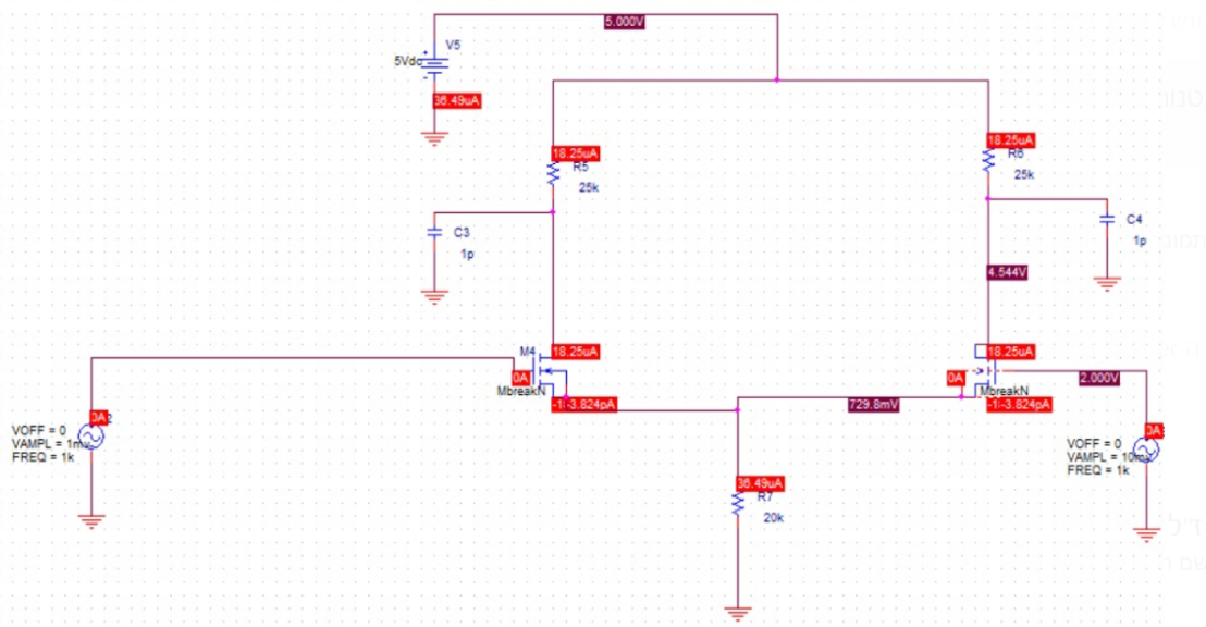
Hello, I have this spice model so that my calculation are done by paper.
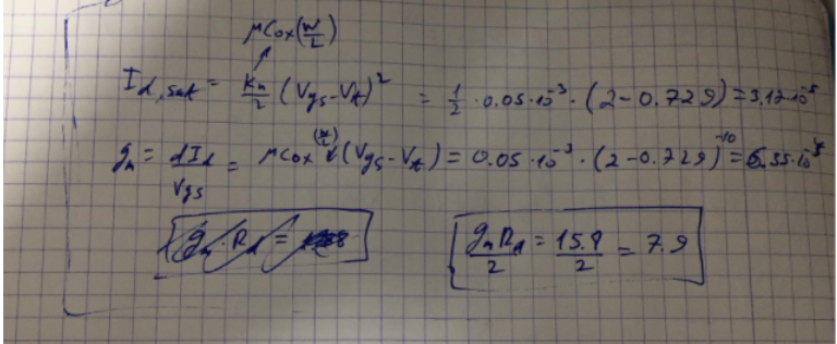
I have made a calculation of the gain as shown bellow.
The Vdc offset is two volts for the bias point.
The gain should be 7.9 but instead its 0.55.
Where did i go wrong?

.model Mbreakn NMOS VTO=1 KP=0.05m W=2.5u L=0.25u
1611935567118.png


1611935648364.png


1611935778777.png
 

The long-tail pair is tricky to find a good operating point. The transistors need to be biased sufficiently so they turn on. If one transistor conducts more, then it causes the other to conduct less (and vice versa).

Looking at your schematic it is unclear whether your mosfets receive sufficient positive bias voltage to turn them on. Run individual tests on the left half and right half of your circuit to see if each side functions as class A amplifiers. As a general rule the greater the ohm value in the emitter leg, the less gain you get. (Your schematic shows a very high ohm value.)

Try applying negative voltage at the tail resistor. This has the same effect as raising bias voltage.

Also try various values for the tail resistor.

At some point you should see the mosfets conducting sufficiently. You should see one influence the other, so that the circuit functions as a differential detector.
 

Status
Not open for further replies.

Part and Inventory Search

Welcome to EDABoard.com

Sponsor

Back
Top