Continue to Site

Welcome to EDAboard.com

Welcome to our site! EDAboard.com is an international Electronics Discussion Forum focused on EDA software, circuits, schematics, books, theory, papers, asic, pld, 8051, DSP, Network, RF, Analog Design, PCB, Service Manuals... and a whole lot more! To participate you need to register. Registration is free. Click here to register now.

Differential pair impedance in PCB stack up

engr_joni_ee

Advanced Member level 3
Joined
Nov 3, 2018
Messages
750
Helped
2
Reputation
4
Reaction score
4
Trophy points
18
Activity points
6,228
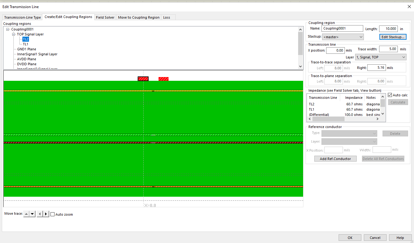
I am running pre-layout simulation in HyperLynx tool. I have shared transmission line editor in the attachment. There is an option "Edit Stackup" on the right top. I also shared the picture of stackup in the attachment.

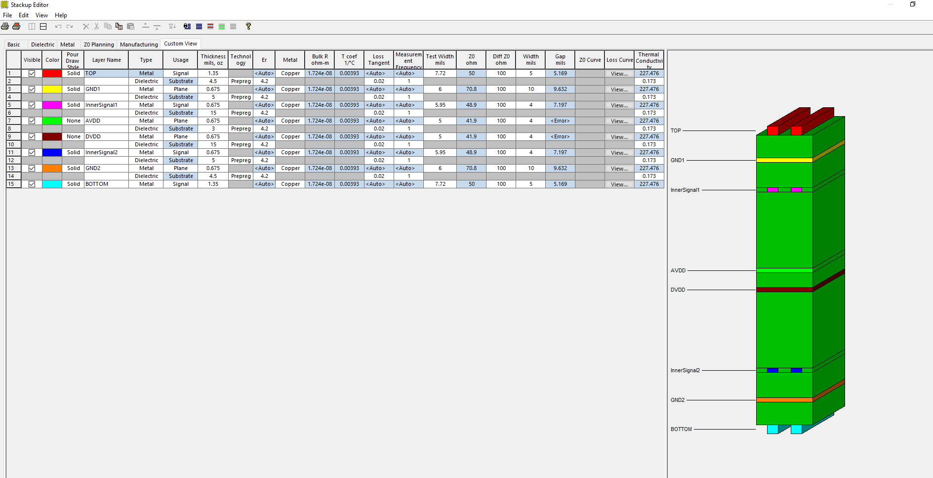
In the stackup editor I have Top, GND1, InnerSignal1, AVDD, DVDD, InnerSignal2, GND2, Bottom. This is eight layer stackup.

On the top layer and I have 50 ohm impedance for single ended signals with a trace width 7.72 mil. The same in true for bottom layer.

For differential signals on the top layer, I have 100 ohm impedance for trace width 5 mil and gap 5.16 mil.

I have one differential pair in the transmission line. If I chose trace width 5 mil and gap 5.16 mil for differential pair on the top layer. The differential impedance is 100 ohm but the single ended impedance is 60.7 ohm which I am worried about.

Do we also need to have exactly 50 ohm impedance for each individual trace in differential pair ?
Untitled 406.png


Untitled 407.png
 
The lumped geometry of Zo=√(L/C) relies mainly on the length/width ratio of the conductors for L and the facing area/gap ratio of the dielectric between the conductors.

Unlike round wire pairs in a shield, the differential of a rectangular strip is not the sum of each wire impedance to ground. This means the Cu base weight and plating thickness matters for the inductance and the Dk matters for C.
You are pointing to an important technical detail. I am afraid, I am not getting it complete. Can you please explain a bit more and also answer to my question asked in the first post. Thanks in advance.
 
Your result is correct for what was given. Single ended is more than half of the differential Zo.,

The ratio of differential/single for Zo is not 2 ( between 1 to 2) and depends on all the dimensional ratios that affect L & C. which includes the plated thickness of the conductor for L and the tolerance of Dk, (unless TDR electrically tested by board shop with defined results using a test coupon outside perimeter)

I assume you know how magnitude of impedance is defined for L(f) & C(f).
 
Last edited:
The differential impedance is 100 ohm but the single ended impedance is 60.7 ohm which I am worried about.

Do we also need to have exactly 50 ohm impedance for each individual trace in differential pair ?
You'll have 50 ohm individual impedance if the lines are completely separated, but that's not the idea of a differential pair.

Read about even and odd impedance of differential pair.
 
Yes, I got the concept of even and odd impedance. Referring to the stackup in post #1, the even mode impedance is around 60 ohm and odd mode impedance is 100 ohm for transmission line to Top layer.

What are the consequences if the even mode impedance is not 50 ohm in differential pair ?

Referring to the stack up in post #1, the stackup is not symmetric, the reference planes for InnerSignal1 (layer3) are GND1 (layer2) and AVDD (layer 4) and the plane height for InnerSignal1 (layer3) is not same which we can see that the GND1 (layer2) and AVDD (layer 4) have different height. Is it necessary to have same height of reference planes in stripline transmission line ? What are the consequences if the height of reference planes is not same in stripline transmission line ?
 
Zeven of 100 ohm differential TL can be between 50 ohm (lines uncoupled) and several 100 ohms (no ground present).
As stated, most differential TL are closely coupled and Zeven is respectively higher, e.g. 70 to 120 ohm. Zeven has no effect on differential signals, some signal standards, e.g. full speed USB use additional single ended signalling and have specifications for common mode impedance respectively Zeven.
Is it necessary to have same height of reference planes in stripline transmission line ?
Generally not. You want substrate heights in a similar range for compact stackup implementation, but it's not always possible. You can play with Saturn PCB toolkit to evaluate different embedded transmission line configurations.

1698405097482.png
 
I see there are four terms, Zeven, Zodd, Zdifferential, Zo in Saturn tool. I am not sure that difference between Zdifferential and Zo in Saturn tool. I am using 8.31.

My understanding about Zeven and Zodd was that.

Zeven is the single ended impedance when p and n have same singles running on them. In this case each single ended signal has ground reference which is the plane under. In other words, the return path for each p and n signal is running on the ground reference which is the plane under.

Zodd is the differential impedance when p and n have opposite polarity singles running on them. In this case the reference of p line is n line. In other words the return path of p signal follows n signal which is opposite in polarity.
 
The meaning of Zeven and Zodd is explained in literature. E.g. Pozar Microwave Engineering has been suggested in a previous discussion. ZO is referring to the impedance of single conductor as explained in Saturn toolkit help.
 

LaTeX Commands Quick-Menu:

Part and Inventory Search

Welcome to EDABoard.com

Sponsor

Back
Top