Continue to Site

Welcome to EDAboard.com

Welcome to our site! EDAboard.com is an international Electronics Discussion Forum focused on EDA software, circuits, schematics, books, theory, papers, asic, pld, 8051, DSP, Network, RF, Analog Design, PCB, Service Manuals... and a whole lot more! To participate you need to register. Registration is free. Click here to register now.

Differential MOS amplifier

Status
Not open for further replies.

furiaceka

Newbie level 3
Newbie level 3
Joined
Jul 3, 2013
Messages
4
Helped
0
Reputation
0
Reaction score
0
Trophy points
1
Visit site
Activity points
31
Hi,
I have this type of circuit to analyze:
Schermata 2013-07-03 alle 16.39.33.png
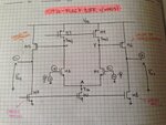
1) What is the kind of topology of this circuit? because it is similar to a OTA fully diff but there are 2 differential pairs(M7-M8 and M1-M2), one with Vo and another with differential and common input
2) What is the differential gain Ad?

if you have any link with explanation of this circuit I'm very happy to read it.
 

Hi,

This is a simple 2 stage filly differential Opamp.
Input at the gates of M1-M2 and Output across RL.

There is only one differential input pair, M1-M2.

M1-M2 is the input transistors with M3-M4 as the current source load. The current is defined by the bias circuit involving M9-M10 and Ib.

M7 and M8 is the current source load for the second stage. The second stage input pair is M5-M6.

The gain for the first stage would be
A1 = 2 x gm-1,2 x (ro-1,2||ro-3,4)

The gain for the second stage would be
A2 = 2 x gm-5,6 x (ro-5,6||ro-7,8)

Total gain would be the product of the individual stage gains.

Thank you for your fast reply.
So it' equal to this other circuit: (the only difference is that M5,M6 are pMos instead of nMos, what is change??)
IMG_1264.JPG

So in this case the total differential gain is:

ATOT = 2 x gm1 x (ro1||ro3) x gm5 (ro5||ro7)

it's correct?

Thanks in advance
 

Sorry but I didn't notice that M5-M6 were NMOS in the first circuit. In that case the second stage would not have any gain since it is just Source follower(buffer). Therefore the total gain would be the gain of the first stage alone.
Also the first circuit does not have any common mode rejection.

The second circuit is indeed a proper OTA with common mode rejection because of the tail current in the first stage. The equation for gain given by you is also correct.

PS the circuit diagram for the 2nd circuit shows that the inputs are given without any common mode unlike in the 1st circuit with Vc+Vd/2 and Vc-Vd/2. But the 2nd circuit would also require a minimum common mode for the circuit to operate.
 

Sorry but I didn't notice that M5-M6 were NMOS in the first circuit. In that case the second stage would not have any gain since it is just Source follower(buffer). Therefore the total gain would be the gain of the first stage alone.
Also the first circuit does not have any common mode rejection.
Ok thanks!
So M5-M6 is a source follower to optimize the transfer of energy to load, and M7-M8 are the biasing transistor of the source follower stage.
It is correct?


The second circuit is indeed a proper OTA with common mode rejection because of the tail current in the first stage. The equation for gain given by you is also correct.
PS the circuit diagram for the 2nd circuit shows that the inputs are given without any common mode unlike in the 1st circuit with Vc+Vd/2 and Vc-Vd/2. But the 2nd circuit would also require a minimum common mode for the circuit to operate.

yes it is only a sketch that I use to calculate the output range, but I know that a Vcm is needed!

Thanks for your patience and for your help.
 

Status
Not open for further replies.

Part and Inventory Search

Welcome to EDABoard.com

Sponsor

Back
Top