Continue to Site

Welcome to EDAboard.com

Welcome to our site! EDAboard.com is an international Electronics Discussion Forum focused on EDA software, circuits, schematics, books, theory, papers, asic, pld, 8051, DSP, Network, RF, Analog Design, PCB, Service Manuals... and a whole lot more! To participate you need to register. Registration is free. Click here to register now.

different outputs from 2 pack buffer IC

DNA2683

Advanced Member level 4
Joined
Sep 3, 2012
Messages
106
Helped
0
Reputation
0
Reaction score
0
Trophy points
1,296
Activity points
2,290
Hi Guys,

I've been working on a circuit design that involves two input signals passing through buffers before entering a differential op-amp. I'm currently facing an issue with the steady-state behavior of the circuit. When I apply an input of 0V to both of the buffers (or tie both inputs to GND), I expected to see 0V (or perhaps a few millivolts) on both of the buffer outputs. However, for some reason, I'm observing different output voltages from the two buffers.

It's important to note that these buffers are part of the same IC package. I'm puzzled by this behavior, as I expected the outputs to be identical when both inputs are the same.

The buffers I'm using are TI TLV9062. To help you better understand the circuit, I've attached a diagram outlining the concept.

Could anyone provide insights or information on what might be causing this issue? Your assistance in resolving this matter would be greatly appreciated.
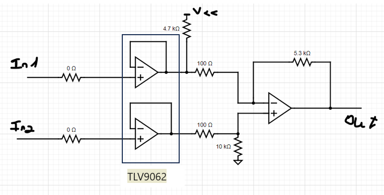
1697177211940.png
 
Hi,

I guess the problem is mainly
* the power supply
* combined with the output_low_voltage behaviour (specification).

Your description misses some important informations:
* power supply voltages for all the Opamps
* how are the supplies connected
* power supply bypass capacitors
* what is the most right Opamp type? If also a dual (multi) Opamp, how is the remaining Opamp connected?
* PCB layout ... needed to verify if you followed the layout recommendations
* if you complain about "different voltages" the tell us the actual voltages. Otherwise it's meaningless for us. We don't know whether you talk about 1mV, 10mV, 100mV or 1V.

Klaus
Thanks kalus for you quick response

I'm using a 3.3V with 100nF capacitors , all AMPs feeds from the same 3.3V and GND.
the voltage that i get from the buffer output is 10 mV( the one that connects to the - on the op amp) and the other one 8mv- thats why the - is wining on the op amp.
the op amp is a TI TLV2333
the output of the opamp connected to another buffer and go to MCU A2D
i dont have the layout on my computer i will try to get it

TNX!!!
 
Hi,

8mV and 10mV is quite better than I expected.

I mean they are specified to go down to 20mV/60mV to GND. So why complaining at all?

It´s simple physics that an OPAMP can´t pull the output beyond it´s power supply rails. (typical OPAMP without special features)
Indeed no OPAMP can pull exactly to the rail - not even a so called "rail-to-rail" OPAMP. There always is a gap.
With non "rail-to-rail" types the gap may be some volts. With "rail-to-rail" types the gap is much smaller in the region of several 10mV.

Now look at your schematic.
The upper OPAMP´s output is pulled externally to VCC (I ask myself: why at all). The OPAMP needs to fight against it to pull it to GND. It it does a good job in this.
But the lower OPAMP´s output already gets externally pulled to GND. Thus the OPAMP does not to do anything to get the output to GND.

So - to be honest - your circuit is badly designed. A good design never goes to the very limit.
There are some possible solutions (focussed on the buffers):
* either use a negative power supply (my recommendation)
* or add a bit of offset to both buffers. The added offset should be equal to both paths. So the difference between them does not change. The input to the difference amplifier still is perfect.

****
Tbh: with a total gain of about 50 .. I ask myself why you don´t use a dedicated instrumentation amplifier....or why you don´t design it like an instrumentation amplifier. --> differential gain mainly at the input stage than on the output stage.

Klaus
 
The resistor dimensioning looks arbitrary-wrong. The purpose of the 4k7 resistor is questionable, it increases minimal output voltage, you'd better use a pull-down if you want output near zero.

In case the output stage is intended as difference amplifier, it should use symmetrical resistors, e.g. 10k + 10k for gain of 100. Unfortunately the output range is cplamped to positive differences In2 > In1. If you want symmetrical difference, output should be centered to Vcc/2.
 
Hi,

8mV and 10mV is quite better than I expected.

I mean they are specified to go down to 20mV/60mV to GND. So why complaining at all?

It´s simple physics that an OPAMP can´t pull the output beyond it´s power supply rails. (typical OPAMP without special features)
Indeed no OPAMP can pull exactly to the rail - not even a so called "rail-to-rail" OPAMP. There always is a gap.
With non "rail-to-rail" types the gap may be some volts. With "rail-to-rail" types the gap is much smaller in the region of several 10mV.

Now look at your schematic.
The upper OPAMP´s output is pulled externally to VCC (I ask myself: why at all). The OPAMP needs to fight against it to pull it to GND. It it does a good job in this.
But the lower OPAMP´s output already gets externally pulled to GND. Thus the OPAMP does not to do anything to get the output to GND.

So - to be honest - your circuit is badly designed. A good design never goes to the very limit.
There are some possible solutions (focussed on the buffers):
* either use a negative power supply (my recommendation)
* or add a bit of offset to both buffers. The added offset should be equal to both paths. So the difference between them does not change. The input to the difference amplifier still is perfect.

****
Tbh: with a total gain of about 50 .. I ask myself why you don´t use a dedicated instrumentation amplifier....or why you don´t design it like an instrumentation amplifier. --> differential gain mainly at the input stage than on the output stage.

Klaus
Thanks Kalus, very detailed explanation and insights.
I don't have a lot of flexibility since I already have the board. So changing the voltage to negative or use instrumental Amp.
But if you say that the 4.7k pull up on the upper buffer can make this buffers output bit different . Maybe I will recover this resistor will help the buffer to get closer to 0V as the lower buffer output.

WDYT? Is it worth to try or I'm in a dead end?

Many thanks for your help
 
Hi,

Both FvM and me mentioned that the function of the 4k7 is unclear.
Maybe you could enlighten us.

Klaus
 
In addition, it would be useful to know intended input voltage range and expected transfer function. Is the asymmetrical gain intentional?
 
Sim :

1697290953401.png


The sim shows pullup increases that OpAmps output by (318.03 - 317.74) or ~ 250 nV.
Thats with 0V VG1, at -5V its ~ double.

Thats with exact value R's as shown. All bets are off if you are using 1% or worse R's.
And of course the Vos, AOL, PSRR differences between OpAmps will affect.


Regards, Dana.
 
Last edited:
Insights will come after you define some basic specs.

Vin range:____ DC, AC , fmax
Vcm in: ___ ( incl. interference DC, AC)
Source Impedance:_____
V+ : 3.3V

Diff Gain: ___
CMRR : ____
Vo Offset: ___ max

Purpose: ___________

What results would you get with these simple changes which should be obvious?
1697291847397.png

Problems:
1. 5.3k/0.1k Resistor mismatch in your design has reduced the CMRR to -35 dB !!
2. 100 ohms on Vin- side only , presents a virtual load of 100 Ohms will add more differential error when current rises with a differential Vin.

What if you used TLV2333 for all?

Where physically did you use Gnd for your measurements?
Were these measured with a DMM or a scope?

If you have CM noise when signals are near 0V, you need to raise the reference voltage from 0V.
 

LaTeX Commands Quick-Menu:

Similar threads

Part and Inventory Search

Welcome to EDABoard.com

Sponsor

Back
Top