Continue to Site

Welcome to EDAboard.com

Welcome to our site! EDAboard.com is an international Electronics Discussion Forum focused on EDA software, circuits, schematics, books, theory, papers, asic, pld, 8051, DSP, Network, RF, Analog Design, PCB, Service Manuals... and a whole lot more! To participate you need to register. Registration is free. Click here to register now.

Different Characteristic of NMOS device in FF and FS corner

Status
Not open for further replies.

niteshtripathi

Member level 3
Joined
Oct 11, 2013
Messages
59
Helped
0
Reputation
0
Reaction score
0
Trophy points
6
Activity points
429
Hi all,

As we know in FF and FS (corner notation), first letter corresponds to the NMOS device while the second with PMOS device.

While characterizing only NMOS device, I found that Id vs Vds plot is different for FF and FS while it should be same because in both corners the NMOS is Fast only.

Any leads will be helpful. thanks.
 

Hello niteshtripathi!

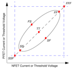
First, take a look at this picture:

Screenshot from 2017-07-24 17-50-44.png

From this picture, you can see that the 'fast' for FF and FS corners are not at the same coordinate.
So you can not expect that FF and FS for the n-type lead to the same results. :)
This is because the FS is a mixed mode corner so it does not take the full variations of the fast-fast or slow-slow process corners.
I hope my explanation was enough for you, but if not, you can check the model guide of the technology you are using for further information.
Plus, you can take a look at https://edadocs.software.keysight.com/display/iccap2012/Introduction+to+Corner+Modeling
Best regards.
 
Hi, Thanks for sharing the info.


Hello niteshtripathi!

First, take a look at this picture:

View attachment 140095

From this picture, you can see that the 'fast' for FF and FS corners are not at the same coordinate.
So you can not expect that FF and FS for the n-type lead to the same results. :)
This is because the FS is a mixed mode corner so it does not take the full variations of the fast-fast or slow-slow process corners.
I hope my explanation was enough for you, but if not, you can check the model guide of the technology you are using for further information.
Plus, you can take a look at https://edadocs.software.keysight.com/display/iccap2012/Introduction+to+Corner+Modeling
Best regards.
 

This is useful to know.

Following the same argument - does it mean, that FF/SS corners do not consider the full variation of nMOS and pMOS devices?
I.e., while corners like TF, TS, ST, FT are not usually considered, the F and S variations in these corners should be larger than their variations in FF / SS corners - correct?
 

Hmm.. I am not sure whether I understood your question correctly or not.
In general, standard CMOS process has 5 corners (FF, FS, SS, SF and TT).
FF and SS take into account full variation of both nmos and pmos.
Basically the VT and Idsat changes in both devices to match fast (for FF) or slow (for SS) circuit delay as measured on ring oscillators during inline testing.
Therefore, if I understood correctly, I suppose the corners you mention by TF, TS and so on, should NOT have larger variations than FF/SS corners.
Just as a matter of curiosity the FFF and SSS are called functional corners and they are used in some technologies.
A “functional corner” is defined as a group of corner parameter values that will predict the +/- 3-sigma limit of a critical electrical parameter, such as Idsat or Vtsat.
Functional corners put extreme Idsat and Vt for wide and narrow short channel FETs.
In this case, it is more "severe" than FF and SS corners, but not all technologies use this.
 

Yes, I know about these five corners, but these corners is just an approximation of a real life, where both nMOS and pMOS devices have some spread (Vt, Id,...), with some correlation between them.

Thanks for explaining the "functional" (more extreme) corners.

I thought a little more about this, and I think I agree with you.
It is because of the correlation between nMOS and pMOS (for example, Vt for both will be lower and Idsat higher for thinner gate oxide), that the extreme corner will happen at FF, and not TF or FT.

Thank you!
 

Status
Not open for further replies.

Part and Inventory Search

Welcome to EDABoard.com

Sponsor

Back
Top