Continue to Site

Welcome to EDAboard.com

Welcome to our site! EDAboard.com is an international Electronics Discussion Forum focused on EDA software, circuits, schematics, books, theory, papers, asic, pld, 8051, DSP, Network, RF, Analog Design, PCB, Service Manuals... and a whole lot more! To participate you need to register. Registration is free. Click here to register now.

[SOLVED] Diff amp and Vbe Multiplier problems

Status
Not open for further replies.

webald0

Newbie level 6
Joined
Mar 7, 2013
Messages
14
Helped
0
Reputation
0
Reaction score
0
Trophy points
1,281
Activity points
1,408
First, i wanna say hello :) this is my first post, i have this problems in my head for few weeks now so i decided to ask this here.

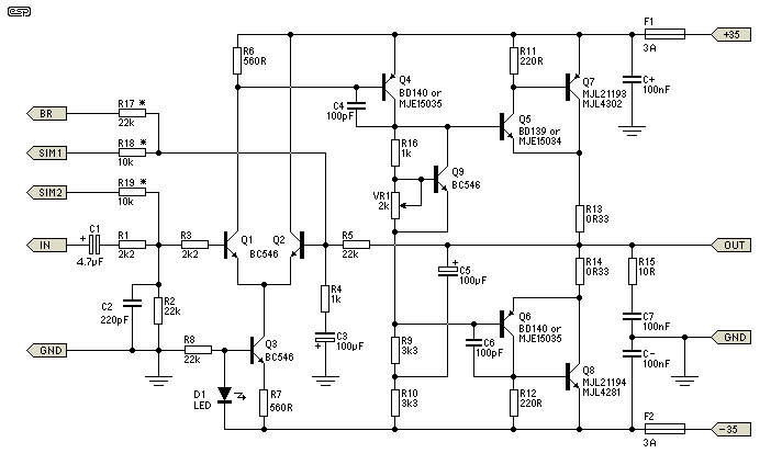
I will construct Rod Elliotts P3A -> **broken link removed**

i am doing this for my college, so i need to do some calculations. First thing is to do a DC analysis, and here is my first problem.
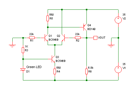
Diff amp Diffamp.jpg

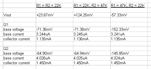
Base resistors are asymmetric, how can i calculate Base currents/voltages?

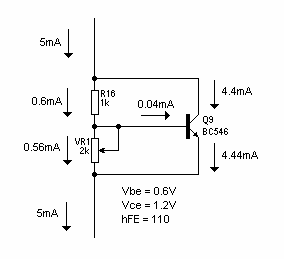
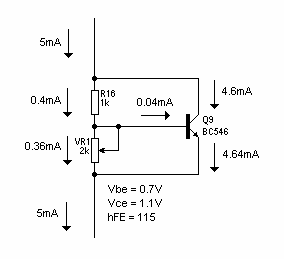
Second problem is Vbe multiplier in VAS part of the amp.

Vbe Multiplier.jpg

How to calculate emmiter and base current of Q4?

Thank you very much for answers, if more parameters are needed ill put them as soon as i can.
 

how can i calculate Base currents/voltages?
As a rule of thumb, the voltage between base and emitter is about 0.6V.

In theory base current = collector current / hFE.
In practice you can forget about doing any accurate calculation of base current, because you don't know what the hFE is. For example the BC546 datasheet says it's hFE could be anywhere between 110 and 800 at 25 degrees centigrade with collector current = 2mA. Just to make things more interesting, hFE changes with temperature and collector current as well, as the graph below shows.


Btw, if you look at a datasheet from a different manufacturer, you may see a totally different looking graph. That's because the "same" part from different manufactirers aren't actually the same.

Anyway, the point is that "assume beta = 100" only happens in classroom exercises, not real life.

Having said all of that though, the situation's not completely hopeless since we normally don't care what the base current is anyway, so long as it's low enough to not cause a problem.

What we can do is a sort of "worst case" analysis, to calculate the highest value the base current might be. For example a BC546 with Ic = 1mA should have an hFE of at least 100, so base current should be less than about 10uA. We dont know whether it's 10uA or 2uA, but we do know it's not more than about 10uA.

First thing is to do a DC analysis.....
Good thinking. Let's start with the voltage gain stage and Vbe multiplier, referring to the schematic below (which I copied from your link, so I hope it's the right one).


For the given supply voltage, the current through R9 and R10 is about 5mA. This is also Q4's collector current, and the current flowing through the Vbe multiplier.

Looking at the Vbe multiplier: To bias the output stage correctly, Q9 must have about 1.2V between collector and emitter, i.e. about 0.6V across each of R16 and VR1. So VR1 will be set to about 1K and there will be about 0.6mA flowing through R16 and VR1.

Since we started with 5mA, the other 4.4mA must flow through Q9. Since Q9's hFE is at least about 110, the base current must be less than about 0.04mA. Since Q9's base current is at least 10 times smaller than the current flowing through R16 and VR1, it doesn't really effect the calculation - we can forget about it.

Moving on to Q4....
Collector current is about 5mA and the hFE is lousy - the datasheet says hFE = 40 to 160 at Ic = 150mA (IIRC), but at 5mA it may be worse. So Q4's base current may be as high as 0.1mA or even a bit more. At the same time Vbe = about 0.6V, so there's about 1mA flowing through R6.

Added together, that means Q1's collector current is probably a bit more than 1mA.

Which brings us (at last) to the input stage and current source.

I don't know exactly what the forward voltage of the green LED is, but it will be high enough to ensure Q3's collector current is more than 2mA. How much more is a bothersome question, but let's assume Rod's done his homework and designed the circuit so so that the collector currents of Q1 and Q2 are roughly equal i.e. about 1 to 1.5mA each.

This time the base currents actually are important, and cause a slight problem.

Q1's base current flows through R2 and R3 causing a small voltage drop across them, while Q2's base current flows through R5 causing a small voltage drop across it.

If those two voltage drops are equal and the Vbe of Q1 and Q2 are the same, then there will be zero DC voltage between the amplifiers output and ground. That's highly unlikely though, so there's going to be some (unwanted) DC voltage across the loudspeaker. Let's try figure out how bad it is:

To start with, according to the datasheet the difference between the Vbe's could be as much as 150mV, even if the currents through Q1 and Q2 are the same. Hopefully it won't be that bad though and there's not much you can do about it anyway unless you want to take time out to measure individual transistors and select matched pairs.

Then there's the voltage drop across the resistors. Since Ic is probably a bit over 1mA each for Q1 and Q2, and hFE may not be much over 100, the base currents could be as high as about 10uA, but may also be much lower. The worst case here is if the base currents are very different.

e.g. If the base current is 10uA for one transistor and 2uA for the other, this will cause a DC offset across the speaker of about 8uA * 22K = 176mV.

That's not bad, but there is something we can do to improve it. Without using matched transistors, the next best thing is to use transistors with higher hFE, i.e. choose BC546B rather than BC546A. The "A" suffix indicates hFE = 110 to 220, while the "B" suffix indicates hFE = 200 to 450. Even better, use BC547C or BC550C, which have hFE = 420 to 800. (BC546 isn't available in the "C" grade).
 
What we can do is a sort of "worst case" analysis, to calculate the highest value the base current might be. For example a BC546 with Ic = 1mA should have an hFE of at least 100, so base current should be less than about 10uA. We dont know whether it's 10uA or 2uA, but we do know it's not more than about 10uA.

I am using Proteus ISIS simulation program (schematics i posted are from proteus), and i calculated (Icq/Ibq) that hFE is about 365 so i`m calculating with that number. Ib1=3.05uA, Ib2=3.9uA. They are in boundaries <10uA :)

For the given supply voltage, the current through R9 and R10 is about 5mA. This is also Q4's collector current, and the current flowing through the Vbe multiplier.Looking at the Vbe multiplier: To bias the output stage correctly, Q9 must have about 1.2V between collector and emitter, i.e. about 0.6V across each of R16 and VR1. So VR1 will be set to about 1K and there will be about 0.6mA flowing through R16 and VR1. Since we started with 5mA, the other 4.4mA must flow through Q9. Since Q9's hFE is at least about 110, the base current must be less than about 0.04mA.

Since Q9's base current is at least 10 times smaller than the current flowing through R16 and VR1, it doesn't really effect the calculation - we can forget about it.

Your calculation is perfect :) but i found a problem here. 5mA is Vbe multiplier, R9,R10 and Q4 collector current. 5mA-0.6mA=4.4mA. But 4.4mA is not flowing through Q9 collector because there is small amount current that goes as base current to Q5. Maybe this is too much asking, but this is one more thing that bothers me, how to get this base current..

I recreated a simulation and made a pic --> Vbe multiplier #2.jpg

Moving on to Q4....
Collector current is about 5mA and the hFE is lousy - the datasheet says hFE = 40 to 160 at Ic = 150mA (IIRC), but at 5mA it may be worse. So Q4's base current may be as high as 0.1mA or even a bit more. At the same time Vbe = about 0.6V, so there's about 1mA flowing through R6.

Added together, that means Q1's collector current is probably a bit more than 1mA.

Which brings us (at last) to the input stage and current source.

I don't know exactly what the forward voltage of the green LED is, but it will be high enough to ensure Q3's collector current is more than 2mA. How much more is a bothersome question, but let's assume Rod's done his homework and designed the circuit so so that the collector currents of Q1 and Q2 are roughly equal i.e. about 1 to 1.5mA each.

it fascinates me how you get all this from head.. :grin: with help from simulation, i calculated hFE of Q4 about 55-60, while Vbe is 0.57V

This time the base currents actually are important, and cause a slight problem.

Q1's base current flows through R2 and R3 causing a small voltage drop across them, while Q2's base current flows through R5 causing a small voltage drop across it.

If those two voltage drops are equal and the Vbe of Q1 and Q2 are the same, then there will be zero DC voltage between the amplifiers output and ground. That's highly unlikely though, so there's going to be some (unwanted) DC voltage across the loudspeaker. Let's try figure out how bad it is:

To start with, according to the datasheet the difference between the Vbe's could be as much as 150mV, even if the currents through Q1 and Q2 are the same. Hopefully it won't be that bad though and there's not much you can do about it anyway unless you want to take time out to measure individual transistors and select matched pairs.

Then there's the voltage drop across the resistors. Since Ic is probably a bit over 1mA each for Q1 and Q2, and hFE may not be much over 100, the base currents could be as high as about 10uA, but may also be much lower. The worst case here is if the base currents are very different.

e.g. If the base current is 10uA for one transistor and 2uA for the other, this will cause a DC offset across the speaker of about 8uA * 22K = 176mV.

Voltage drops on R2+R3 and R5 are not the same due to simulation, and Ib`s are not very different -> Ib1=2.98uA, Ib2=3.78uA while hFE is about 365

one more pic :D ----> Diffamp #1.jpg

Ill try to configure my question as best as i can with my sloppy english :) so:

Lets suppose that Base resistors are the same, and the Base currents are the same. When i raise resistance of one side (therefore, currents drops on that side and base current on Q2 raises), how to calculate how much has the other current raised? How to get that ratio? Maybe is stupid question, or i don`t understand some obvious or basic things...... :-(

That's not bad, but there is something we can do to improve it. Without using matched transistors, the next best thing is to use transistors with higher hFE, i.e. choose BC546B rather than BC546A. The "A" suffix indicates hFE = 110 to 220, while the "B" suffix indicates hFE = 200 to 450. Even better, use BC547C or BC550C, which have hFE = 420 to 800. (BC546 isn't available in the "C" grade).

I`ll have my eye one this when construction begin. Thank You very much, people take money for instructions like this, You do it for free.. I wish there are more people like You Sir. I am so glad i visited this forum. Thanks once again.

Martin
 
Last edited:

Hi, sorry for the delay

but i found a problem here. 5mA is Vbe multiplier, R9,R10 and Q4 collector current. 5mA-0.6mA=4.4mA. But 4.4mA is not flowing through Q9 collector because there is small amount current that goes as base current to Q5. Maybe this is too much asking, but this is one more thing that bothers me, how to get this base current..
To be honest; when I did the calculation the first time I was sloppy - I didn't bother to figure out whether 4.4mA was the collector current or the emitter current. That's because it doesn't make much difference. Since hFE > 100, there is less than 1% difference between collector current and emitter current, so you get less than 1% error if you calculate the base current using the wrong value.

Strictly Ib = Ic / hFE
or Ib = Ie / (hFE + 1)

Anyway, I worked it out properly now and it turns out 4.4mA actually is the collector current after all, as shown below.


Obviously for higher hFE, the base current will be even lower. The point is that whatever the hFE, the base current will be much lower than the current through the resistor and trimmer, so it won't affect things much - the trimmer will need to be set fairly close to 1K, it's center value.

~~~~~~~~~~~~~~~~~~~~~~~~~~~~~~~~~~

What's more interesting is to consider the effect of different VBEs.
For example, let's assume:
  1. Vbe of the driver transistors in the output stage is less than 0.6V, so we need a total bias voltage across the Vbe muliplier of 1.1V instead of 1.2V.
  2. Vbe of the Vbe muliplier transistor = 0.7V.
  3. Thus Vcb is only 0.4V.
Now the picture is as shown below. Since the voltage across the trimpot is 0.7V and the current through it is 0.36mA, it will have to be turned up almost to the maximum value (2K).


Lets suppose that Base resistors are the same, and the Base currents are the same. When i raise resistance of one side (therefore, currents drops on that side and base current on Q2 raises), how to calculate how much has the other current raised? How to get that ratio?
That's an interesting question.

I suspect you're thinking in terms of the first circuit you showed in post 1, with the resistors from both bases connected to ground. In that case the calculation of what happens if you change one of the resistor's values is quite tricky. (i.e. I'm not tempted to spend the next 1/2 hour trying to figure it out:-D).

Fortunately we don't have to because in the actual amplifier the resistor from the base of the right hand transistor goes to the output of the amp not to ground, and that actually makes things easier.

Remember there's a lot of negative feedback around the circuit, so it's trying very hard to keep the currents through the input transistors constant (and keeping the voltage between their bases constant).

What this means is that when you change the value of the resistors, the voltage across them changes while the base current through them remains almost the same. The amplifier's output voltage changes to whatever value is needed to to keep the currents from changing.

I'll do a sim and post the results to show what I mean a bit later.
 
Last edited:
Hi, sorry for the delay

Why sorry? :D you made me a big favor just with first post. This is a lifetime due for me :)


To be honest; when I did the calculation the first time I was sloppy - I didn't bother to figure out whether 4.4mA was the collector current or the emitter current. That's because it doesn't make much difference. Since hFE > 100, there is less than 1% difference between collector current and emitter current, so you get less than 1% error if you calculate the base current using the wrong value.

Strictly Ib = Ic / hFE
or Ib = Ie / (hFE + 1)

Anyway, I worked it out properly now and it turns out 4.4mA actually is the collector current after all, as shown below.

Yeah i understood how to get that current from your first reply. And i know that base current of Q9 is so small that its irrelevant, but the base current what i need to know is Q5 base current. Because of that Q5 base current, Q4`s collector current won`t be 4.4mA, it will be 4.4-Ib5=? In my simulation Q5`s base current is 0.18mA, but i don`t know how to get that with mathematical equation.


Obviously for higher hFE, the base current will be even lower. The point is that whatever the hFE, the base current will be much lower than the current through the resistor and trimmer, so it won't affect things much - the trimmer will need to be set fairly close to 1K, it's center value.

~~~~~~~~~~~~~~~~~~~~~~~~~~~~~~~~~~

What's more interesting is to consider the effect of different VBEs.
For example, let's assume:
  1. Vbe of the driver transistors in the output stage is less than 0.6V, so we need a total bias voltage across the Vbe muliplier of 1.1V instead of 1.2V.
  2. Vbe of the Vbe muliplier transistor = 0.7V.
  3. Thus Vcb is only 0.4V.
Now the picture is as shown below. Since the voltage across the trimpot is 0.7V and the current through it is 0.36mA, it will have to be turned up almost to the maximum value (2K).

Thanks for this, you made Vbe multiplier role in amplifier much closer to understand now

That's an interesting question.

I suspect you're thinking in terms of the first circuit you showed in post 1, with the resistors from both bases connected to ground. In that case the calculation of what happens if you change one of the resistor's values is quite tricky. (i.e. I'm not tempted to spend the next 1/2 hour trying to figure it out:-D).

Fortunately we don't have to because in the actual amplifier the resistor from the base of the right hand transistor goes to the output of the amp not to ground, and that actually makes things easier.

Remember there's a lot of negative feedback around the circuit, so it's trying very hard to keep the currents through the input transistors constant (and keeping the voltage between their bases constant).

What this means is that when you change the value of the resistors, the voltage across them changes while the base current through them remains almost the same. The amplifier's output voltage changes to whatever value is needed to to keep the currents from changing.

I'll do a sim and post the results to show what I mean a bit later.

I already made a sim and thats 100% true :D . My problem is as always mathematically to get that base currents but now, after few days of trying to figure it out, i figured that its not so important to have this currents so precisely calculated. I know that Ib1<Ib2 (and also Ic1<Ic2) because Rb1>Rb2.
 

Here's a nice simplified circuit. It leaves out the output stage, but models the DC conditions elsewhere quite well.


I tried it first with R1 = R2 = 22K as shown. Then I tried it with first R2 then R1 changed to 47K, to see what difference that makes to the DC conditions. Here's the results:


When I started out, I thought four significant digits would be enough to show the differences. Turns out five digits would have been better for the currents. Drat.

Anyway, it does illustrate the point I was trying to make - when you double the value of either resistor, the base and collector currents only change by about 0.1%, if that.

OTOH, the output voltage changes all the way from from -57mV to +124mV. That's the DC offset across the speaker I was talking about in post 2.

- - - Updated - - -

And i know that base current of Q9 is so small that its irrelevant, but the base current what i need to know is Q5 base current. Because of that Q5 base current, Q4`s collector current won`t be 4.4mA, it will be 4.4-Ib5=?
Oh, OK. More sloppiness on my part - I just ignored that :oops:.

Going by the full schematic in post 2, It's actually Q6 you need to worry about, not Q5. The quiescent current for the Vbe multiplier is set by R9 and R10, and Q6's base steals some of that.

Anyway, here's how to work out the base current for Q5 and Q6:
The trick is to start at the output and work forwards.

Let's start by assuming the collector currents of the output transistors (Q7 and Q8) are both about 100mA. That's actually a fairly safe assumption since the whole point of the trimpot in the Vbe multiplier is that it lets you set the quiescent current in the output stage to 100mA.

Assuming hFE = 50, the base currents of Q7 and Q8 will be about 2mA. But there's also about 3mA flowing through R11 and R12, so the total collector currents for Q5 and Q6 will be about 5mA.

Assuming hFE = 50 again, the base currents of Q5 and Q6 will be about 0.1mA. So the current through the Vbe multiplier will be 4.4mA - 0.1mA = 4.3mA.

BTW: bear in mind that the current through R9, R10 and the Vbe multiplier is proportional to your power supply voltage, and unless you're using a regulated supply that that's proportional to your mains voltage.

In other words, if your mains voltage changes by + or -5%, that "4.4mA" will change by + or -5% too.

In my simulation Q5`s base current is 0.18mA....
I expect you've got the output stage idling current set too high. Either that or hFE is even worse than I used in the calculation above.
 
Thank you very much.. I read it and i think you got all my problems solved :D i`ll calculate it tommorow, today i am out of time. i`ll write here what i got!

thanks once more Sir
 

Here's a nice simplified circuit. It leaves out the output stage, but models the DC conditions elsewhere quite well.


I tried it first with R1 = R2 = 22K as shown. Then I tried it with first R2 then R1 changed to 47K, to see what difference that makes to the DC conditions. Here's the results:


When I started out, I thought four significant digits would be enough to show the differences. Turns out five digits would have been better for the currents. Drat.

Anyway, it does illustrate the point I was trying to make - when you double the value of either resistor, the base and collector currents only change by about 0.1%, if that.

OTOH, the output voltage changes all the way from from -57mV to +124mV. That's the DC offset across the speaker I was talking about in post 2.

Yeah i see it now... I made the whole project simulation and it really is, resistance change doesn`t make any difference. And -57mV to +124mV is ok? As you said in your first post, it can be better but its not too bad either..

Let's start by assuming the collector currents of the output transistors (Q7 and Q8) are both about 100mA. That's actually a fairly safe assumption since the whole point of the trimpot in the Vbe multiplier is that it lets you set the quiescent current in the output stage to 100mA.

I assume i should already know this by now, but i will have a courage (over internet :D) and ask you - why is Vbe multiplier setting output stage to 100mA? How do you know that? By transistor specification or? In proteus, i couldn`t find a MJL21193 transistors used in Rod Elliots P3A so i used MJE350 & MJE340 just for simulation, so i have 300mA in my output stage. Is that because of transistors? If its hard to explain it or you have a lack of time, can you give me only some pointers to find it out myself?
 
Last edited:

i couldn`t find a MJL21193 transistors used in Rod Elliots P3A so i used MJE350 & MJE340 just for simulation,
That's OK.

so i have 300mA in my output stage. Is that because of transistors?
Sort of. Changing the transistors will change the output stage current, even if you swap one transistor for another transistor with the same part number. That's why the trimpot is there - it lets you set the current to the desired value despite the differences between transistors.

Similarly, if you are repairing an amplifier and have to replace any of the output transistors or driver transistors, then you have to re-adjust the trimpot to set the correct current again.

why is Vbe multiplier setting output stage to 100mA?
If the current is set too low, the distortion gets much worse.
If the current is set too high, the distortion may get a bit worse too, but more importantly it's just wasting power and heating up the transistors unnecessarily.

In that article, Rod Elliot recommends setting the output stage current to somewhere between 50mA and 100mA.
 
Once more thank you very much Sir! :D
 

Status
Not open for further replies.

Similar threads

Part and Inventory Search

Welcome to EDABoard.com

Sponsor

Back
Top