Continue to Site

Welcome to EDAboard.com

Welcome to our site! EDAboard.com is an international Electronics Discussion Forum focused on EDA software, circuits, schematics, books, theory, papers, asic, pld, 8051, DSP, Network, RF, Analog Design, PCB, Service Manuals... and a whole lot more! To participate you need to register. Registration is free. Click here to register now.

[SOLVED] designing wide swing cascode current mirror with wide current range

Status
Not open for further replies.

r.mirtaji

Junior Member level 3
Joined
Feb 9, 2020
Messages
27
Helped
0
Reputation
0
Reaction score
0
Trophy points
1
Activity points
403
Dear friends,

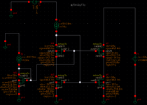
I attached you the picture of the wide swing current mirror and here is my question please,

We know that current mirror sources use to copy current (W / L ratio) from one circuit block to another

without the resistance of the next block affecting this current transfer

The following factors are important to us when designing a current source:
1-Output impedance
2-maximum swing
*3-wide current range

Is it possible to design a wide swing current mirror that the output current follows a wide range of input currents?
The wide swing current mirror is usually designed to produce a constant current with a coefficient relative to the input current.
In the figure below, when the input current is between 4uA and 20uA, all transistors operate in the saturation region.
But when the current is less than 4uA. First, the M4 enters the linear region And at lower currents, the transistors M1,M2,M3 enter the sub-threshold region.

1-Can the circuit be designed that in the lower current all transistors are in the saturation region and the wide swing current mirror has more wide range?
2-Is the operation of the circuit correct even though the transistors are in currents of less than 4 that enter the sub-region and the operation of the circuit is acceptable?
 

Attachments

  • Untitled1.png
    Untitled1.png
    38.6 KB · Views: 920

At some point when you decrease the current, the transistors will have to enter the subthreshold region. This is just the way they work. Also, reducing the current, M4 will go into triode inevitably because the Vgs of M3 becomes smaller.
On the high current side you may hit current values for which Vgs of M3 increases enough to put M3 in linear because its drain voltage reduces since M4 will also need more Vgs as the current increases and if you keep its gate constant. I think if you also increase the current in M5, then the gate of M4 will be increasing with it and the drain of M3 will sort of keep up with the increased current in the diode connected transistors M3 and M4. You should be able to find a combination of current increase rates which keep both M3 and M4 in saturation for max current range.
 
Dear Suta,
I want to use this circuit in output of the DAC This circuit is drawn in the figure below
The output current of DAC varies between 0 and 20uA with a step size of 100nA(LSB)

The circuit I designed when the input current is between 4uA and 20uA, all transistors operate in the saturation region
the current is less than 4uA. First, the M4 enters the linear region And at lower currents, the transistors M1,M2,M3 enter the sub-threshold region
(W/L 1,2,3,4= 4u/1u)
as you said "when you decrease the current, the transistors will have to enter the subthreshold region."
1-What is the best design for this circuit in which the transistors are in the saturated region at the maximum out put of DAC current range?
the maximum out put of DAC current range that i have designed between 4uA and 20uA.
2-Does the circuit work properly for the low currents that the transistors operate in the substation area?
 

Attachments

  • 1.png
    1.png
    101.7 KB · Views: 262

I think the mirror should work well also in subthreshold region. A concern could be matching. Run MC for low currents and see if matching is still good for you. Spede too will degrade at low currents.
If you make M1/3 work with higher Vgs for as small currents as possible and make M3/4 stronger, and with appropriate gate voltage so they don't go in linear too soon as the current decreases, you can find a sweet spot that keeps all devices in saturations for the max current range. Make sure you don't interfere with the headroom needed for everything that's above the current mirrors.
 
Thanks sutapanaki

Suppose we want to design a current source that works in the range of the input current between 1uA <Iin<20uA and all transistors (Tr 1 to 4) work in SAT region.

In Figure 1, we designed an initial circuit that works in the range of the input current between 2.8uA <Iin<20uA with fixed Vbias=635mV and W/L=4u/1u all transistors (Tr 1 to 4) work in SAT region.


In order to make the transistors M1 to M4 work in the saturation region under 2.8uA , we must reduce the W according to the following equation.

\[ Vgs↑ ∝ ( L/W↓) \]

In Figure 2, in order \[ Vgs↑>Vth then W↓=2um \]

In Figure 2, in order for M1 and M2 work in the saturation region when Iin>9uA the bias voltage must be increased as the current (Iin) increases. In other words, the bias voltage follows the changes in the input current.


\[ Iin ↑then Vbias ↑ \]

\[ Iin ↓then Vbias ↓ \]

Question:

By decreasing the W and as a result increasing the Vgs. I could not greatly reduce range of the input current just (figure1: 2.8uA to figure2: 1.5uA) 1.3uA.

Is there a design method to achieve less input current range?

Is there a circuit to generate bias voltage that tracks the input current? Note that our input current source is a digital analog-to-current converter.
 

Attachments

  • 1.jpg
    1.jpg
    240.8 KB · Views: 300

You don't need a super precise voltage for the gates of the casodes. Can you use the dump current from your post #3 to produce a current to bias M5?
 

Thanks sutapanaki
I used the voltage source temporarily, I can use M5 (stack Tr) to creat voltage
My question is this, as I mentioned in the previous post

Is there a design method to achieve less input current range?

Is there a circuit to generate bias voltage that tracks the input current? Note that our input current source is a digital analog-to-current converter.
 

Dear Dominik
Exactly the digital-to-analog converter works in the linear region
the voltage drop at the input terminal of this current mirror is v=vth+vov=.35+.15=>when Iin=20uA
At low currents of DAC, transistors of wide swing current source enter the sub-threshold region
I want to design the current mirror so that the transistors operate at the wide range of input current in the saturation region.
In previous posts, I mentioned the design challenges I faced
I'm looking for the best design for the wide current mirror for this circuit
Do you think it is ok that the input current is between(100n<Iin<20uA LSB=100nA resolution=8bit) and this current mirror works between 2.8 <Iin<20uA in saturation region.
To design this current source in this circuit, which item should I consider the most?(high accuracy, high output impedance,speed,slewrate,etc)
 

In my opinion mirroring DAC current is a mistake.

However, if you really want to do it, the active current mirror is the only solution (any design with opamp).
The main constraint for CM transistors will be matching requirements in case of max current. So with 25.5uA current mismatch has to be below 50nA if you want to keep INL below 0.5LSB. It implies large transistors in this current mirror and really low speed at low currents.
However, if you don't care about INL you can sacrifice it for area and speed.

The best current mirror design in terms of linearity for wide range of current is the one proposed by Teresa Serrano ca 20 years ago. However, it requires opamp which has to handled both input and output current flowing ine the mirror.
 
Status
Not open for further replies.

Part and Inventory Search

Welcome to EDABoard.com

Sponsor

Back
Top