Continue to Site

Welcome to EDAboard.com

Welcome to our site! EDAboard.com is an international Electronics Discussion Forum focused on EDA software, circuits, schematics, books, theory, papers, asic, pld, 8051, DSP, Network, RF, Analog Design, PCB, Service Manuals... and a whole lot more! To participate you need to register. Registration is free. Click here to register now.

design&simulation of electronic ballast

Status
Not open for further replies.

remyatr

Newbie level 2
Joined
Oct 14, 2009
Messages
2
Helped
0
Reputation
0
Reaction score
0
Trophy points
1,281
Location
kerala
Activity points
1,301
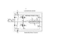
i would like to deign an electonic ballast for flourescent lamps.i would like to include a buck boost power factor correction circuit for the improvement of powerfactor. a series resonant parallel loaded circuit is used to drive the lamp output stage.i would like to switch the circuit using zero voltage switching and i would like to sense the output voltage and according to the change in out put voltage i have to adjust the puls width of the two switches inorder to achieve both same phase for both input volage and current.My circuit is attached below..how can i design such an electronic ballast and how i simulate the same?
corurl=http://obrazki.elektroda.pl/65_1255496626.jpg]
65_1255496626_thumb.jpg
[/url]rection
 

hi, man.
i suggest you to search paper on:
PFC using buck-boost
and
LCC resonant converter.

the application note whitch publiced by IR,Fairchild,ST,Philips...

hope may do some .
 

howcome you choose buck boost with its chopped input current.?

you can get low voltage out but for fluorescent you need high voltyage
 

Status
Not open for further replies.

Similar threads

Part and Inventory Search

Welcome to EDABoard.com

Sponsor

Back
Top