Dymtra
Newbie level 6
Hi, I am designing a CMOS differential amplifier for a course, I must obtain a gain of 20 dB and a cutoff frequency of 100 MHz.
This is the circuit

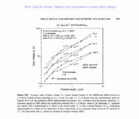
I got my transfer function, and from there my gain is given by , i can see that it's given in terms of the transconductance which i can obtain with width and lenght values, but the other part is given by lambda, which is a parameter that the teacher didn't gave us. Is it too critic to know it for the design?
My cutoff frequency is given by which is also in terms of the channel lenght modulation resistances, and i found it difficult to calculate it without knowing the value of lambda, is there other way?
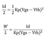
Also the teacher mentioned that the output common mode has to be at least half of Vdd, that would be 1.8V / 2, so I used the saturation current equation to obtain the width and lenght relationship for a value of Vgs = 0.9 V and the half of the current, like this
i don't know if it's ok to make that assumption to obtain the values of width and lenght for the p-MOS.
It would be great to hear your suggestions :smile:
This is the circuit

I got my transfer function, and from there my gain is given by
My cutoff frequency is given by
 which is also in terms of the channel lenght modulation resistances, and i found it difficult to calculate it without knowing the value of lambda, is there other way?
Also the teacher mentioned that the output common mode has to be at least half of Vdd, that would be 1.8V / 2, so I used the saturation current equation to obtain the width and lenght relationship for a value of Vgs = 0.9 V and the half of the current, like this

i don't know if it's ok to make that assumption to obtain the values of width and lenght for the p-MOS.
It would be great to hear your suggestions :smile:
