Continue to Site

Welcome to EDAboard.com

Welcome to our site! EDAboard.com is an international Electronics Discussion Forum focused on EDA software, circuits, schematics, books, theory, papers, asic, pld, 8051, DSP, Network, RF, Analog Design, PCB, Service Manuals... and a whole lot more! To participate you need to register. Registration is free. Click here to register now.

Design current mirror

Status
Not open for further replies.

noor84

Member level 5
Joined
Dec 27, 2017
Messages
90
Helped
0
Reputation
0
Reaction score
0
Trophy points
6
Activity points
688
Hi all,

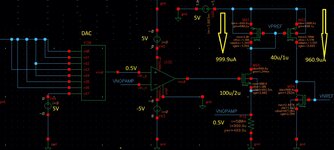
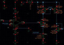
Please, I am going to design the current mirror as in the circuit shown in the attached picture, I have a problem with my circuit that is:
I can not get the same current in the other branch as shown in the picture.
Could you please help me to solve this problem?

Note: the dimensions of W and L for the transistors are shown and I selected them based on trial and error to get these results. Is there any rule to follow to select the best transistor dimensions?


Regards.
 

Attachments

  • Untitled.jpg
    Untitled.jpg
    215.5 KB · Views: 143

Hi there,

What is the minimal L for the MOSFET? It is a good practice to use about 10x Lmin in given technology to minimize channel length modulation, improve the threshold voltage stability (VTH vs L) and minmize the dependency on process variations (MC simulations).

The transistors in current mirror should have the same W/L and number of fingers (if mirroring ratio is 1:1), same VDS above VDS_sat and the inversion (VGS-VTH) as high as possible to mirror the current properly.

Judging by the voltages and currents, you are using rather older CMOS technology and L = 1um might not be enough.... plus your VDS conditions might not be ideal for correct mirroring either, but that is not shown in your picture.

Bruteforce method can be used here, I think... Just set W and L of both transistors as variables. W_M91 = W_M92 = W and the same for length. L_M91 = L_M92 = L = 10x Lmin and step W through the DC / OP analysis. This way you might tune the W/L to your liking....

Shlooky
 
Last edited:

Hi there,

What is the minimal L for the MOSFET? It is a good practice to use about 10x Lmin in given technology to minimize channel length modulation, improve the threshold voltage stability (VTH vs L) and minmize the dependency on process variations (MC simulations).

The transistors in current mirror should have the same W/L and number of fingers (if mirroring ratio is 1:1), same VDS above VDS_sat and the inversion (VGS-VTH) as high as possible to mirror the current properly.

Judging by the voltages and currents, you are using rather older CMOS technology and L = 1um might not be enough.... plus your VDS conditions might not be ideal for correct mirroring either, but that is not shown in your picture.

Bruteforce method can be used here, I think... Just set W and L of both transistors as variables. W_M91 = W_M92 = W and the same for length. L_M91 = L_M92 = L = 10x Lmin and step W through the DC / OP analysis. This way you might tune the W/L to your liking....

Shlooky

Hi shlooky,
Thank you for your reply,

What is the minimal L for the MOSFET?
I am working on 0.18um technology.

It is a good practice to use about 10x Lmin,
I tried to maximize the L but I have to maximize the W also, and I don't want to be the transistor too big. and I am already using 1um for L.


The transistors in the current mirror should have the same W/L and number of fingers (if mirroring ratio is 1:1), same VDS above VDS_sat and the inversion (VGS-VTH) as high as possible to mirror the current properly.
I am training to do this but I can not. why? I don't know how!!


Judging by the voltages and currents, you are using rather older CMOS technology and L = 1um might not be enough,
I don't understand your view point on older CMOS technology.


plus your VDS conditions might not be ideal for correct mirroring either, but that is not shown in your picture.
See the attached new picture please,


Bruteforce method can be used here, I think... Just set W and L of both transistors as variables. W_M91 = W_M92 = W and the same for length. L_M91 = L_M92 = L = 10x Lmin and step W through the DC / OP analysis. This way you might tune the W/L to your liking....
I am a beginner in using Cadence, and honestly, I dont know how? I am changing manually.

I hope to get answer.
regards.
 

Attachments

  • 2 Untitled.jpg
    2 Untitled.jpg
    143.6 KB · Views: 112

Hi,

The picture you posted confirms my point. Voltage conditions are not ok.
Looks like your M92 is in linear regime... VGS = 3.599V, but your VDS = 5 - 1.401 = 2.6V.
Both devices need to be saturated....

I was not expecting 5V and 1mA in 180 nm CMOS, but if those are thick oxide devices, no problem at all...

You can type in a variable name instead of numeral value for W or L. For example width would be equal to "foo" and length will be "goo". Check&Save.
Then in simulator window (ADE) you go "Variables -> Copy From Cellview" and set a default values for foo and goo. Say 10u and 1u.

If everything is correct, you can run basic simulations with these variables. If you are happy, then you go

"Tools -> Parametric Analysis", set up min and max values, number of steps, etc. and fire that one off.
If you set everything correctly, ADE will iterate your basic analyses with stepped variable according to your settings.

The simplest example is the output characteristics of MOS transistor. You want to DC sweep VDS of your MOSFET, but step VGS to get multiple curves in one waveform window....

Shlooky
 
Last edited:

Hi,

The picture you posted confirms my point. Voltage conditions are not ok.
Looks like your M92 is in linear regime... VGS = 3.599V, but your VDS = 5 - 1.401 = 2.6V.
Both devices need to be saturated....

I was not expecting 5V and 1mA in 180 nm CMOS, but if those are thick oxide devices, no problem at all...

You can type in a variable name instead of numeral value for W or L. For example width would be equal to "foo" and length will be "goo". Check&Save.
Then in simulator window (ADE) you go "Variables -> Copy From Cellview" and set a default values for foo and goo. Say 10u and 1u.

If everything is correct, you can run basic simulations with these variables. If you are happy, then you go

"Tools -> Parametric Analysis", set up min and max values, number of steps, etc. and fire that one off.
If you set everything correctly, ADE will iterate your basic analyses with stepped variable according to your settings.

The simplest example is the output characteristics of MOS transistor. You want to DC sweep VDS of your MOSFET, but step VGS to get multiple curves in one waveform window....

Shlooky
Thank you for your reply,
=============================================
The picture you posted confirms my point. Voltage conditions are not ok.
Looks like your M92 is in linear regime... VGS = 3.599V, but your VDS = 5 - 1.401 = 2.6V.


The transistor M92 is in Sat: VSD>VSG-abs(Vth) ===>
(5-3.99=2.601)> (5-1.401)-abs(1.178)=2.421
then 2.601>2.421 (Sat), also the cadence shows that this transistor is sat (region 2).
=================================================
Please, what can I do now? I checked all transistors and the transistors are in Saturation, but till now I didn't get the same currents.

Regards.
Hi, Try doing cascoding between M92 and M94, This should help
 

Status
Not open for further replies.

Similar threads

Part and Inventory Search

Welcome to EDABoard.com

Sponsor

Back
Top