Continue to Site

Welcome to EDAboard.com

Welcome to our site! EDAboard.com is an international Electronics Discussion Forum focused on EDA software, circuits, schematics, books, theory, papers, asic, pld, 8051, DSP, Network, RF, Analog Design, PCB, Service Manuals... and a whole lot more! To participate you need to register. Registration is free. Click here to register now.

Design an Isolated SMPS with multiple output

Status
Not open for further replies.

Prototype21

Junior Member level 1
Joined
Mar 3, 2020
Messages
15
Helped
0
Reputation
0
Reaction score
0
Trophy points
1
Activity points
121
Hello Guys, l Iike to design a AC to DC Isolated Switching Power Supply with multiples outputs with 3v3, 5v, 24v with 300mA each with optocoupler. I using a starter schematic attached below, but I don´t know how I can rewire it for multiple output with 3v3, 5v, 24v with 300mA. Need some help guys!!

eda.png
 

For starters, the optocoupler is backwards.
It should be LED to the right side, and phototransistor to the left.

Also you would use multi tapped secondaries, because otherwise your linear 5V and 3V3 regulators would be dissipating more power than what they are delivering.
 
I can't see the primary side working at all well - the main transistor is not turned off appropriately (?) - there is cktry missing ...
 
  • Like
Reactions: FvM

    FvM

    Points: 2
    Helpful Answer Positive Rating
Hi,

The title says "isolated", but the schematic shows "non isolated".
What's your AC input voltage?

******

I wonder what's the idea behind that starters do it the hard way...design all discrete from the scratch....without detailed tutorial.

* There are many thousands, maybe millions proven circuits in the internet.
* If you just don't want to copy: There are application notes that explain how it works and how to calculate it..in detail, step by step.
* If one wants to keep it simple (and modern): There are ICs that include most of the circuitry inside... with datasheets, with simple explanations how to keep function stable and reliable

I assume no professional (who never designed an SMPS before) would go this way....because high development time and failures are expectable. At least I would not do it this way.
I compare it with building a car without modern techniques, using a steam machine instead of a modern motor. Using a steam machine, but never really learned how a steam machine works.

Don't get me wrong. I don't want to discourage anyone from making his own experience.
I just want to be true. This project may cause disappointment, maybe even losing the fun in designing electronics.

My recommendation: Keep it simple, go small steps.
Thus with each small step you have your own sense of achievement, keeping you motivated.
I'd start with small, non isolated, step down circuits to generate 3.3V and 5.0V from 24V, that you later can use with the isolating SMPS circuit.

Some additional hints:
* SMPS generally can not be (usefully) tested on a breadboard. You need a PCB with a solid GND plane.
* In case of AC input is mains voltage: If you are not experienced with dangerous voltage design, "creepage distance" and "clearance" ... please be very careful not to harm yourself or others. Then I recommend to buy an AC_in 24V_DC_out supply to keep it safe.

Klaus
 

if you ignore the extraneous gnd/earth symbols and the opto swapped left to right - then it is isolated - as plainly intended ....
 

I wonder what's the idea behind that starters do it the hard way...design all discrete from the scratch....without detailed tutorial.
Hi, KlausST. I just want to learn. Thats why i choose the hard way. I know its tough but lets see.

For starters, the optocoupler is backwards.
It should be LED to the right side, and phototransistor to the left.

Also you would use multi tapped secondaries, because otherwise your linear 5V and 3V3 regulators would be dissipating more power than what they are delivering.

I can't see the primary side working at all well - the main transistor is not turned off appropriately (?) - there is cktry missing ...

Thanks so much for the response guys, I inverted the phototransistor and swap the transformer as mentioned. But I don´t know, how a I dimensioning the flyback return, because now I have 3 outputs. I imagine I need 3 more flybacks, one each for output.

I calculated any secundary spirals each 30% turn plus
L1 = 100 turns
L2 = 3 turns
L3 = NC
L4 = 4 turns - 3,3v
L5 = 6 turns - 5v
L6 = 28 turns - 24v

The regulators I use for shortcut protection!

image.png
 

Hi,

I know its tough but lets see.

Paralleling the diodes usually doesn´t work sataisfactory. This is because of production tolerance and thermal drift you may expect that the one diode carries 80% while the other only 20%. (more or less)
The problem is, that the power distribution acts like an avalange: The one with the higher current will become hotter --> the hotter one becomes lower impedance and thus carries even more current.
Mounting on a big common heatsink will only slightly improve this.

Paralleling diodes does not considerably increase efficiency either. Voltage drop is almost the same, current stays the same, thus P = V x I is almost constant. --> loss is almost constant. Efficiency is almost constant.

But I see efficiency is not your target at all, otherwise you won´t use linear regulators with 30% voltage overhead.

Klaus
 

The primary ckt is still way wrong ( look at it closely ) paralleling diodes is often used in switch-modes as it is not DC, the pulse waveshape of the current pulses in the diodes goes a long way to ensure balanced operation - even better to have them close together and on the same heatsink ... equal length leads ...

- - - Updated - - -

Also it would be better to have one tightly regulated 24VDC o/p then a buck to 5v1 then a buck to 3v3 - much better overall efficiency .... and the 3v3 will then be very stable - as will the 5v1
 

Thank you for the response guys. I am trying to build the schematic just only with PTH components. A Buck circuit I will need some SMT components which I cant buy at this point of time.
 

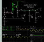
The key is to achieve snap action of the control device. A home-brew switch-coil converter does not require a commercial IC. Control can be done by op amp, logic gate, or two transistors arranged so gain is multiplied. These change state quickly in response to a slight change at the input.

Example, invert-gate senses load voltage dropping below supplyV/2 (adjustable by potentiometer). It goes high, turning on transistors. When load V rises above supplyV/2 the gate goes low.

This method is able to control 24V supply using IC's which cannot endure more than 15V.

buck converter controlled by invert-gate bias NPN bias PNP 24 VDC to 5V 300mA.png

The 100pF capacitor is an integrator causing slight delay in changes at the input. This introduces hysteresis in the action.
 
Status
Not open for further replies.

Part and Inventory Search

Welcome to EDABoard.com

Sponsor

Back
Top