Continue to Site

Welcome to EDAboard.com

Welcome to our site! EDAboard.com is an international Electronics Discussion Forum focused on EDA software, circuits, schematics, books, theory, papers, asic, pld, 8051, DSP, Network, RF, Analog Design, PCB, Service Manuals... and a whole lot more! To participate you need to register. Registration is free. Click here to register now.

Dependence of Parasitic of MIM cap on substrate contact resistance

Status
Not open for further replies.

ktx2222

Member level 5
Joined
Jan 8, 2014
Messages
81
Helped
2
Reputation
4
Reaction score
2
Trophy points
8
Activity points
613
Hi everyone,

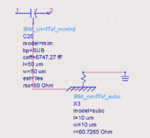
I have one question about the dependence of parasitic of MIM cap on substrate contact resistance. I am using IBM pdk. I found that the parasitic of MIM cap in this process strongly depends on substrate contact. Please take a look at attached image:
2014-03-09 6-39-48 PM.png

The parasitic of cap is very small if the subc is set to 10 kOhm (default resistance of subc). However, if subc is set to 60 Ohm by increasing the area of subc (as indicated in photo), the parasitic of MIM cap becomes significant. I don't know the effect of subc in a full circuit. How many subcs/How much area of subc should I put in the real layout? Am I right if I put only one subc in a layout to have small parasitic of MIM cap?
Please help me.
Thank in advanced.
 

You need a lot of subc contacts in your full layout: every NMOS needs one or more subc contact(s) near its source, p+ guardrings need a lot of them.

But I don't think you need any subc contact near to a MIM cap.
 
What the substrate capacitance's resistance is, can
affect subtler things like settling time - more resistance
may blow out that settling tail beyond the cycle period
or something like that, while a stiffer tie-down will make
the error capacitance more immediately and strongly felt,
but overwith sooner.

Seen this on old polysilicon substrate SOI, where we had
to dope the poly to lower resistivity to get acceptable
DAC settling times. In RF you generally prefer high resistivity
substrate, so high that the bottom plate to substrate is
invisible at frequencies of interest. At GHz with nice
repetitive waveforms you can play that game; in the
time domain looking for analog accuracy by end of cycle,
you have to worry about time constants making sense
(you either want them way shorter, or way longer than
your period, if you can - either overcome by the local
loop, or ignorable, but not incompletely dealt with).
 
You need a lot of subc contacts in your full layout: every NMOS needs one or more subc contact(s) near its source, p+ guardrings need a lot of them.

But I don't think you need any subc contact near to a MIM cap.

Thank erikl,

I think I can understand the meaning of substrate contact right now. You're right, I don't need to put subc near to a MIM cap. However, because I'm using low resistivity substrate, so I guess other subcs of FET will affect to parasitic of cap. Thank for your advice again, erikl.

What the substrate capacitance's resistance is, can
affect subtler things like settling time - more resistance
may blow out that settling tail beyond the cycle period
or something like that, while a stiffer tie-down will make
the error capacitance more immediately and strongly felt,
but overwith sooner.

Seen this on old polysilicon substrate SOI, where we had
to dope the poly to lower resistivity to get acceptable
DAC settling times. In RF you generally prefer high resistivity
substrate, so high that the bottom plate to substrate is
invisible at frequencies of interest. At GHz with nice
repetitive waveforms you can play that game; in the
time domain looking for analog accuracy by end of cycle,
you have to worry about time constants making sense
(you either want them way shorter, or way longer than
your period, if you can - either overcome by the local
loop, or ignorable, but not incompletely dealt with).

Thank dick_freebird,

You're right, I'm using low resistivity substrate. I chose this option because I didn't know any concept of high/low resistivity substrate. Now I got some knowledge from you. I guess the high resistivity substrate option may be more expensive than low one? Thank again.
 

Status
Not open for further replies.

Part and Inventory Search

Welcome to EDABoard.com

Sponsor

Back
Top