Continue to Site

Welcome to EDAboard.com

Welcome to our site! EDAboard.com is an international Electronics Discussion Forum focused on EDA software, circuits, schematics, books, theory, papers, asic, pld, 8051, DSP, Network, RF, Analog Design, PCB, Service Manuals... and a whole lot more! To participate you need to register. Registration is free. Click here to register now.

DC simulation error Cadence - 2 nodes have unreasonable voltage

Status
Not open for further replies.

melkord

Full Member level 3
Joined
May 18, 2018
Messages
151
Helped
0
Reputation
0
Reaction score
1
Trophy points
18
Activity points
1,767
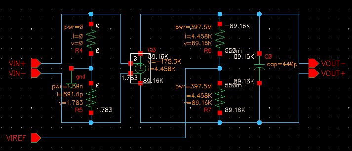
I have tried to change the gmin to a smaller value and try to check the gmin-check option. the problem is still there.

This ideal amp instance is used also in another circuit and the simulation works ok.
The problematic nodes drive the Gate of MOSFETs.

What simulation option I have to check to solve this issue?
1599755844978.png


Code:
Opening the PSF file ../psf/dc.dc ...
Important parameter values:
    reltol = 100e-06
    abstol(V) = 1 uV
    abstol(I) = 1 pA
    temp = 27 C
    tnom = 27 C
    tempeffects = all
    gmindc = 1 pS
Trying `homotopy = gmin'.

Notice from spectre at Vtgc = 1.8 during DC analysis `dc'.
    GminDC = 1 pS is large enough to noticeably affect the DC solution.
        dV(I13.I53.M2.m1:int_d) = -34.6437 mV
        Use the `gmin_check' option to eliminate or expand this report.
    Bad pivoting is found during DC analysis. Option dc_pivot_check=yes is recommended for possible improvement of convergence.
Warning from spectre at Vtgc = 1.8 during DC analysis `dc'.
    WARNING (CMI-2375): M17.m1: Vgs has exceeded the oxide breakdown voltage of `vbox' = 11.7 V.
    WARNING (CMI-2377): M17.m1: Vgd has exceeded the oxide breakdown voltage of `vbox' = 11.7 V.
    WARNING (CMI-2375): M18.m1: Vgs has exceeded the oxide breakdown voltage of `vbox' = 11.7 V.
    WARNING (CMI-2377): M18.m1: Vgd has exceeded the oxide breakdown voltage of `vbox' = 11.7 V.
Notice from spectre at Vtgc = 1.79 during DC analysis `dc'.
    GminDC = 1 pS is large enough to noticeably affect the DC solution.
        dV(I13.I53.M2.m1:int_d) = -34.6435 mV
        Use the `gmin_check' option to eliminate or expand this report.
    Bad pivoting is found during DC analysis. Option dc_pivot_check=yes is recommended for possible improvement of convergence.
 

Kiloamps and mavavolts is usually a sign that
something's bent.

Can this particular vcvs be assigned some clip
limits to keep voltage from swinging out past sane
operation? I know some simulators include limit
properties for controlled sources, whether the
analogLib vcvs has and passes such properties
I do not recall.

Maybe something like a vccs and burden resistor
with stop-diodes, followed by a unity gain vcvs,
could give you a better bounded response if no
local-clip option is accessible for the one you are
currently using.
 

You use VCVS and this element ideal and \[ V_{out+} \] and \[ V_{out-} \] are probably open circuit and there is no DC return path for VCVS.
Right ??
Connect a high valued ( 1 MegOhm) resistor to GND because SPICE based simulators don't like this kind of floating or No_DC_Return_Path configurations
 

Voltage at VIN- is 1.783, while at VIN+ is 0. With vcvs gain in order of 100dB it is not unusual to get 180kV in a circuit.

The issue is with circuit one level up in hierarchy (maybe there is no negative feedback?). You are mentioned it is driving mosfet gate - Common source configuration inverses signal phase, so to achieve negative feedback, drain has to be connected to positive input of opamp, instead of negative.

One of the solution is to provide borders for vcvs output voltage to supply values.
vcvs has such properties like min/max output voltage, simply set these quantities to 0 and vdd.
 

Status
Not open for further replies.

Part and Inventory Search

Welcome to EDABoard.com

Sponsor

Back
Top