Continue to Site

Welcome to EDAboard.com

Welcome to our site! EDAboard.com is an international Electronics Discussion Forum focused on EDA software, circuits, schematics, books, theory, papers, asic, pld, 8051, DSP, Network, RF, Analog Design, PCB, Service Manuals... and a whole lot more! To participate you need to register. Registration is free. Click here to register now.

dc-dc converters using PWM as feedback

Status
Not open for further replies.

=DD

Newbie level 4
Newbie level 4
Joined
Dec 1, 2013
Messages
6
Helped
0
Reputation
0
Reaction score
0
Trophy points
1
Visit site
Activity points
47
Hi all,
the attachment shown my circuit drawing,
that one is a zeta converter can increase or decrease output voltage by adjusting duty cycle using PWM as the feedback.
but i cant get the correct result.
would like to ask is there any wrong with the circuit?
the mosfet i dont know which to use p-type or n-type, and how should it connect.

For the PIC I set port d as input, port c output, as I know pin 16 and pin 17 is for PWM connection right?
Is the way I connect the feedback to PIC correct?
hmm maybe my coding have problem too.
but I guess first of all I have to get my circuit right ...

appreciate a lots if any of you could help
=D

**broken link removed**
 

oops sorry
here the attachment

dc dc converter.jpg
 

This looks like a buck converter, correct?

If so then Q2 belongs where R3 is.

I believe L1 and C4 should reverse places. Although they are not absolutely necessary, they interact in a way to create stable current drain from the DC power supply.
 

hi BradtheRad
actually most of converter circuits look almost the same, except the way of components arrangement..
that one is zeta converter, I guess it is not that common ..
hmm ..confusing
 

An internet search turned up this article about zeta converters:

https://www.ti.com/lit/an/slyt372/slyt372.pdf

By changing the duty cycle, you can step the power supply voltage up or down, without inverting the polarity. (The buck-boost type is similar but it inverts the polarity.)

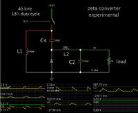
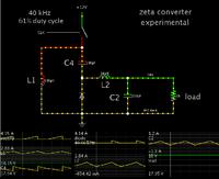
I made a simulation resembling your schematic. (I cannot be certain how vital it is to use a coupled inductor).

12V stepped down to 6 V or so.


12V stepped up to 18V.

C4 must carry 2 or 3 amperes each cycle. It needs to have low ESR.


hi BradtheRad
thanks for the effort=)
I have read before the zeta article link that you provided.
yeah! about the stimulation 12V stepped up to 18V is the correct output if according to the formula shown in the link which is Vout= [D/(1-D)] Vin.
However for 12V stepped down to 6 V, I calculated if D= 0.18 , the output should be 2V..
between I am using Proteus to do the drawing, what do you use for the switching?
as for me I got to use mosfet. But facing problem using it.
any idea?
 

However for 12V stepped down to 6 V, I calculated if D= 0.18 , the output should be 2V..

The step down resulted in a low duty cycle, such that the coil discharged completely and was idle for a time. Hence the converter operated in discontinuous conduction mode (DCM). The normal formula cannot be used in that case.

I am using Proteus to do the drawing, what do you use for the switching?
as for me I got to use mosfet. But facing problem using it.
any idea?

My above simulation (post #6) used a non-existent component called an analog switch. It streamlines the process, so we don't have to complicate our minds with uncertainties of biasing, conduction, etc.

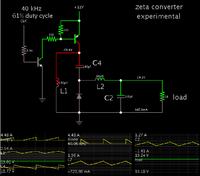
Here is my simulation with a PNP transistor at the high side. It is activated by an NPN, in an arrangement that guarantees the PNP bias will be pulled to a high enough voltage level to turn it off completely.


I tried a P-mosfet, but I have found that Falstad's simulator does not always turn mosfets on sufficiently, whereas it does do so with transistors.

What about using an N-device as the switch? It is common to have to increase its bias voltage so that it will operate at the high side (near the positive supply). But there is something else going on which is unexpected. Notice the volt level on the node below the switching device. It goes to a negative volt level, about the same amplitude as the output voltage. This will make it necessary to finagle with the bias voltage constantly, so that the N-device switches on and off completely. This means it is more practical to use a P-device instead.
 

hi BradtheRad
I tried the drawing on post #8
but the output still extremely low.
I tried to connect that to PIC instead of clock,
facing the same output too.
ahhh, hoping I can get the output right:cry:

- - - Updated - - -

hi FvM,
what did you mean level conversion ?
 

what did you mean level conversion
An active circuit involving transistors or ICs that translates the output level of the processor to the gate voltage level required by the respective circuit.
 

hi BradtheRad
I tried the drawing on post #8
but the output still extremely low.

Can you get a look at what waveform is going through your coil? The coil is the heart of the action.

In my simulation, I adjusted the clock frequency and duty cycle, so that the coil will have sufficient current going through it.

The control network is the difficult part. My simulation does not show that.

You must apply a high enough bias voltage to a P-mosfet (or PNP transistor) in order to fully turn it off.
If your micro puts out 5V, and your power supply is 12V, then the P-mosfet will not fully turn off.
 

Hi FvM
So is it I need an extra active circuit to drive the mosfet?
I have no idea about this. Perhaps can you help?=)

Hi BradtheRad
I changed mosfet to IGBT.
I get the waveform as the attachment.
but the output voltage as you can see is zero :-?
actually I get the same waveform even I use mosfet.
Will it be better if I use IGBT instead of mosfet?
 

Attachments

  • waveform.jpg
    waveform.jpg
    372.5 KB · Views: 72

You're making things worse by using a N-channel IGBT. (IGBT are a bad choice for a low voltage chopper anyway).

My suggestion, stay with a P-channel MOSFET and use a driver similar to Brad's post #8 BJT circuit, but with the MOSFET in place of the output transistor. Resistor values can be later adjusted for optimal MOSFET operation.
 

Status
Not open for further replies.

Part and Inventory Search

Welcome to EDABoard.com

Sponsor

Back
Top