Continue to Site

Welcome to EDAboard.com

Welcome to our site! EDAboard.com is an international Electronics Discussion Forum focused on EDA software, circuits, schematics, books, theory, papers, asic, pld, 8051, DSP, Network, RF, Analog Design, PCB, Service Manuals... and a whole lot more! To participate you need to register. Registration is free. Click here to register now.

DC Blocking capacitor -- How does it know where ground is?

Status
Not open for further replies.

AnalogNewb

Junior Member level 1
Joined
Jul 4, 2010
Messages
17
Helped
0
Reputation
0
Reaction score
0
Trophy points
1,281
Activity points
1,457
Hi Everyone,

A DC blocking capacitor removes any DC offset from an input signal. I've been doing this for years without thinking about it.

My question is, how does it know what the local ground potential is?

My only thought on this is that the output side of the cap is just pushing and pulling electrons, and it adds to / subtracts from whatever the voltage on the input to the circuit already is.

With an inverting op-amp input, it's going into the "virtual ground" of the circuit so that sort of makes sense.

But now I am using a DC blocking cap to feed something that's not an op-amp: an ADM3491 differential line receiver.

So again, how does the cap know where ground is?

Thanks.
 

When you feed a non-DC balanced logic signal to an AC-coupled receiver, neither the blocking capacitor nor the receiver actually can "know where ground is". Even a resistor bias network won't help if the logic signal decides to stay at '0' or '1' for some period. Some signals simply aren't suited for AC coupling.
 

When you feed a non-DC balanced logic signal to an AC-coupled receiver, neither the blocking capacitor nor the receiver actually can "know where ground is". Even a resistor bias network won't help if the logic signal decides to stay at '0' or '1' for some period. Some signals simply aren't suited for AC coupling.

This signal is Manchester encoded and is explicitly intended to pass through pro audio gear, which is all AC coupled. The same question applies equally to sine waves or audio signals.

I know that the capacitor doesn't "know" (it can't) but somehow the circuit as a whole does. I'm assuming this has to do with the input impedance of the circuit after the blocking cap.
 

This signal is Manchester encoded
That's good! You should add a bias network, that sets the idle level to the mid of the receiver's common mode range, unless your sure that it's intended for AC coupled operation.
 

That's good! You should add a bias network, that sets the idle level to the mid of the receiver's common mode range, unless your sure that it's intended for AC coupled operation.

The signal is an industry standard, I'm not generating it.

Can anyone answer my actual question? The AC-coupled signal swings on either side of zero. How does the circuit know where zero volts is?
 

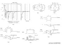
It should be understood that the voltage across a capacitor cannot change instantaneously – current must flow to charge the capacitor and this takes time. It is often necessary to think about current flows in order to understand circuit operation. Also from Fig.1 it is evident that the voltage vC across C and vout across R must add up to vin. Consider a CR circuit (Fig.1) with a voltage step function input. We assume for now that the input step risetime is short compared with the time constant tau=RC of the circuit (if it is not then the output is more difficult to determine, but see the references below). If the step is say vin+ then the output step will also be vin+. If the step remains at +vin for some time then the capacitor will charge exponentialy via R until the output reaches common. If the time with vin at vin+ is less than many times the time constant then the output will be at some level between vin+ and common. If then there is an input step vin back to common i.e. we have a pulse input (i.e. step up then step down) then the ontput signal for the negative going input edge will be a downward step starting from wherever the output is on its exponential response to the original vin+, following which there will be a similar exponential rise towards common (see Fig.2):

Fig.3 shows some simulated results for input pulses of various multiples of the time constant tau.

If the input is a series of pulses then the average level of the output must always be at common since no z.f. is transmitted, but the baseline from which the pulses start will depend on the mark-space ratio (see Fig.5). The d.c. (or more appropriately zero frequency z.f.) level of the input is immaterial since all z.f. information is removed for the output by the C connection. Thus for the output each succeeding pulse sits on the tail of the previous. For a simple case (Fig.5) where tau>>T then ignoring the slight slopes on the pulses the output will appear as shown, with the two shaded areas equal to ensure the average output is at common. If the input pulses arrive randomly in time or in amplitude (or both), then the baseline of the output pulses will vary and this baseline shift can be a serious problem in such circumstances. For more extended discussions see:

Hamilton S (2007) An Analog Electronics Companion (Cambridge University Press ISBN 0780521687805), section 3.7, p206. This book includes the student version of PSpice which will allow you to simulate the pulse response. Plot both voltages and currents to see charging of the capacitor.

Millman J, Taub H (1965) Pulse, Digital, and Switching Waveforms, McGraw-Hill, Capter2.

It should be noted that there is no absolute potential, only potential differences. There is nothing special about comon/ground. Thus an alternative view may be taken if we move the common node from point D to point A in Fig.1, to give Fig.4. Nothing has been changed other than the point from which we measure the potentials. The circuit may now look more familiar as charging C through R. It is also useful to remember that current flows in loops (as shown in the figures) and that it flows through capacitors, not into them. Since the input pulse in Fig.1 is positive going i.e. in Fig.1 point A goes positive relative to point D then in Fig.4 point D goes negative relative to point A, as illustrated in Fig.6. The capacitor C now begins to charge via R so the potential at B changes (exponentially) as shown. The output potential is given by Vout = VBVD and so taking the difference, and allowing for polarities, we get the output waveform shown in Fig.6 i.e. identical to Fig.2.
Prof78.
 
  • Like
Reactions: nafn

    nafn

    Points: 2
    Helpful Answer Positive Rating
Status
Not open for further replies.

Part and Inventory Search

Welcome to EDABoard.com

Sponsor

Back
Top