Continue to Site

Welcome to EDAboard.com

Welcome to our site! EDAboard.com is an international Electronics Discussion Forum focused on EDA software, circuits, schematics, books, theory, papers, asic, pld, 8051, DSP, Network, RF, Analog Design, PCB, Service Manuals... and a whole lot more! To participate you need to register. Registration is free. Click here to register now.

DC blocking cap and post cap DC bias design and layout

Status
Not open for further replies.

AllenD

Member level 5
Joined
Aug 7, 2017
Messages
91
Helped
0
Reputation
0
Reaction score
0
Trophy points
6
Activity points
1,193
Hi Team
I am trying to design a DC blocking cap to only couple my AC signal from the first stage to the second stage of my amplifier.
Can I ask a few questions? I am thinking using the most simple RC topology with a diode connected NMOS to supply the DC voltage, as in the picture.
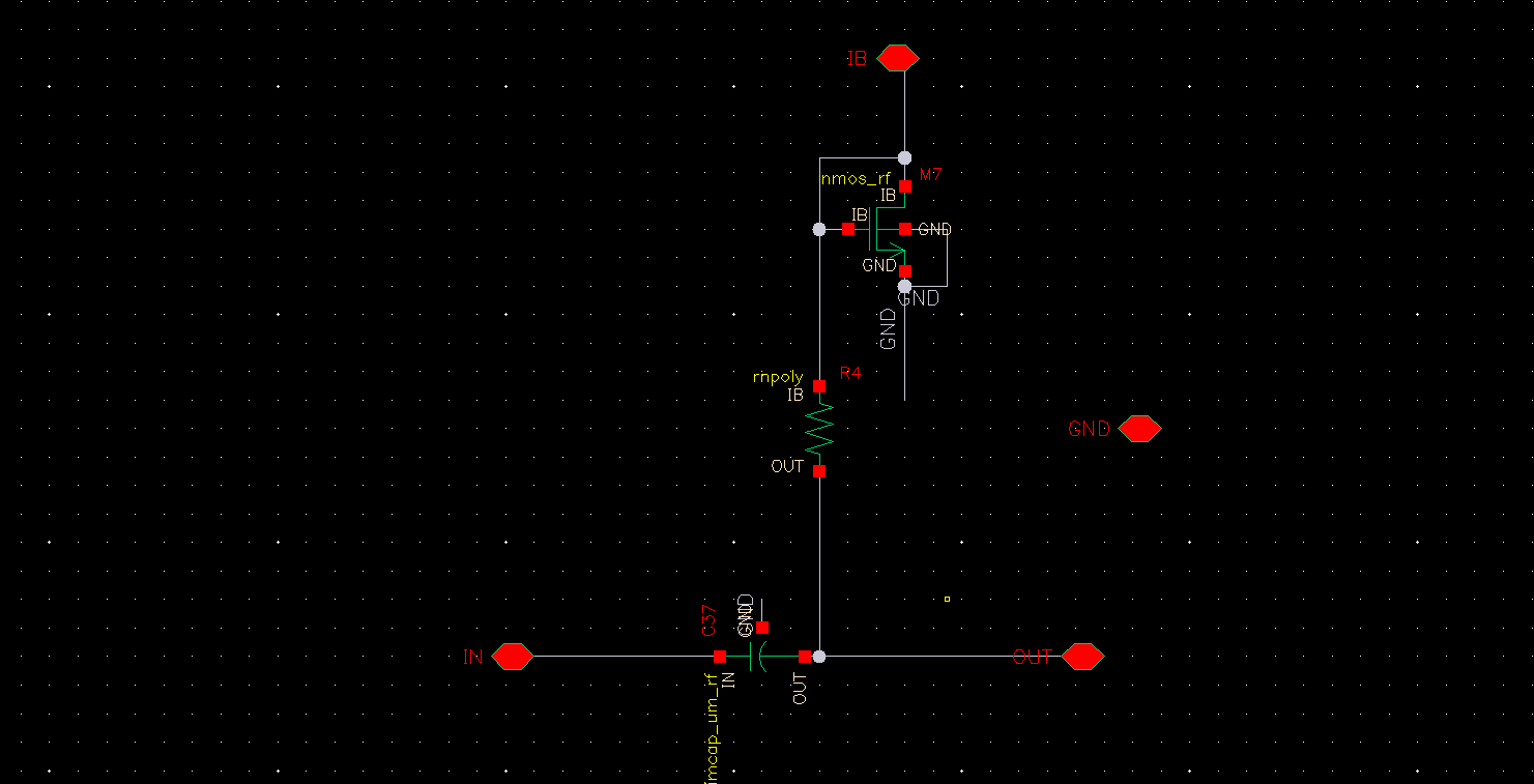
Screenshot from 2021-07-19 12-04-14.png


Assuming the frequency of my coupled AC signal is 1GHz, I know I want the C to be large enough as an AC short and the R large enough to offer a DC voltage at the OUT terminal but not interfere the AC signal at the OUT terminal. But Can you please tell me how should I choose the minimum R and C values? Is there any rule of thumbs to go?

Also, regarding the layout. The C I can use is from M5 and above. and R I can use is R-poly. For a relative big RC, both of them are consuming a lot of die space. Is it a good practice to layout them overlapping? And since there is no trace from M1 to M4 (R is on poly layer and C is M5 and above), should I route some signal traces in between?

Thanks
Al
 

If the predecessor stage has its output common-mode
position fixed, and the successor stage has its input bias
already, then the blocking cap is just a cap.

If you need to bias the successor stage then a MOS-diode
reference and a high value resistor as shown might do.
Whether the MOS-diode voltage is the bias level you
want, who knows?

1K and 1pF would be something like your 1GHz corner,
so probably at least 10X on one or the other, probably
the unsilicided poly resistor (if available) might be best
for density. Size of 1pF cap depends on working voltage,
may be manageable. With so many metal layers you
could consider interdigitated MOM caps as well I guess,
though these are harder to get good process control
(not a WAT control-point) you might be able to use
the route as the capacitor (a few hundred um of
side-by-side, over-and-under traces adds up).
 

This biasing scheme is called 'AC coupling'. There is a logical procedure to go about designing it. Each and every parameter can be calculated with proper logic.

Let's start: Frequency of operation is 1GHz referred as 'fo'. We want the high pass (series C- shunt R) corner frequency to be at least 10x lower to the fo, lower the better. It depends on how much loss is ok for you. Otherwise the high pass nature would create more loss into the input signal. If the RC cut off is to be 100MHz, there are infinite combinations of R and C that result in the same corner frequency. So, how do you choose?

The answer is, the values you choose for R and C have a direct impact on the noise and the signal gain of the circuit.
1. Signal gain: The C will create capacitive division with the input gate cap of the NMOS (whatever your 'OUT' node is connected to). So, you want a higher C so that the capacitive division term is close to unity.
2. Noise: Since the poly resistance is in shunt, its current noise matters. A lower resistance would add higher noise to the noise spectral density at node 'OUT'. You can do noise analysis to confirm it.

So, you want higher C to improve signal gain (minimize signal loss), which will lower the required R for the same RC cut off --> increases noise. So it is a trade off between noise and tolerable signal loss.
 

Status
Not open for further replies.

Part and Inventory Search

Welcome to EDABoard.com

Sponsor

Back
Top