jpm
Newbie level 2

Hello!
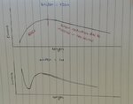
I am current running some simulations on Hpsice and Virtuoso. The simulation consists of nothing more than an on nmos transistor from a 65nm library. The transistor is powered in the threshold regime at 250mV. I am sweeping the length and width and measuring the current through the transistor. My issue is that the results don't fully match what I was expecting to see. I apologise in advance for the crudity of this diagram:

When the width is at the minimum possible (120n), the current rises from the minimum length (60n) due to the Reverse Short Channel Effect and then, after peaking, begins a steady decline due to the increase in resistance of the channel. This is exactly what I suspected.
However, when the width is increased, something I cannot explain begins to occur. At the minimum length, a current peak starts to rise. At around 500n, this surpasses the peak between the RSCE and the linear resistance region. The lower sketch shows the response at 1u.
Can anyone explain why this current peak appears? Is there some physical effect that I am unaware of causing this effect?
I am current running some simulations on Hpsice and Virtuoso. The simulation consists of nothing more than an on nmos transistor from a 65nm library. The transistor is powered in the threshold regime at 250mV. I am sweeping the length and width and measuring the current through the transistor. My issue is that the results don't fully match what I was expecting to see. I apologise in advance for the crudity of this diagram:

When the width is at the minimum possible (120n), the current rises from the minimum length (60n) due to the Reverse Short Channel Effect and then, after peaking, begins a steady decline due to the increase in resistance of the channel. This is exactly what I suspected.
However, when the width is increased, something I cannot explain begins to occur. At the minimum length, a current peak starts to rise. At around 500n, this surpasses the peak between the RSCE and the linear resistance region. The lower sketch shows the response at 1u.
Can anyone explain why this current peak appears? Is there some physical effect that I am unaware of causing this effect?
Last edited:

