kanmaedexandzelbladex
Member level 1

- Joined
- Jul 20, 2013
- Messages
- 35
- Helped
- 1
- Reputation
- 2
- Reaction score
- 1
- Trophy points
- 8
- Location
- Philippines
- Activity points
- 479
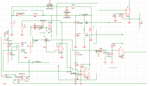
Hello everyone, I seem to have a problem with my fixed off-time current-mode boost converter. The problem is it cannot regulate at its level of 46V with 50kHz switching frequency at max duty cycle operation. I tried to trace the problem and it seemed like it is noise/spikes which causes the duty cycle to not be at the expected level. I have uploaded waveforms below:
Blue = Vgs of mosfet switch waveform, Yellow = Current Sense Waveform (current passing through mosfet switch times sense resistor)
NewFile15 shows what is happening. As can be seen, the Vgs waveform alternates between a long ON-time, and a series of very short ON-times. I think this is false-triggering that is occurring. The only way for the IC to turn-OFF in a current-mode control is for the current sense pin to reach reference. My boost converter output voltage in that condition is at 44.89V. So after the fixed off-time, the IC tries to output ON but the current sense spike may have caused the false turn-OFF. The supply of my IC is connected to an external supply which I am sure is set to a fixed value.
The ON-time shown is a duty cycle clamp (or, an ON-time clamp for fixed off-time). So what happens is the ON-time clamps itself to 21us that's why it is not regulating but I have checked through open loop testing that it doesn't need that amount of ON-time to regulate. It only needs 15us (at full load). If I remove the ON-time clamp, it will regulate at 46V but the Vgs waveform looks still like that but with a longer ON-time.
I have tried lead-edge blanking https://www.edn.com/design/analog/4333114/Circuit-provides-leading-edge-blanking but I used a comparator LM311 instead of an NPN BJT. As can be seen in NewFile15, during the ON-time of the IC, the current sense starts with a 0V "blank". That is my lead-edge blank operation but I was not able to remove completely the spike. This is possibly due to delay of the comparator? I have also implemented this with a breadboard and lots of jumper wires and connectors so it's possible this is due to delay that those wires provide?
I tried putting an RC lowpass filter of about 160kHz cutoff frequency right before the current sense signal enters my IC pin. NewFile22 shows the result and the output voltage improved. Instead of 44.89V, it is steady at 45.4V. That is why I think this is due to false-triggering of IC due to switching spikes. Trying to lower the cutoff frequency of the RC lowpass does not seem to improve it anymore.
I am planning to fabricate a controller daughterboard to remove the issues with delays, parasitics, etc. However, I am not sure if that will fix the problem so I ask for some suggestions? Maybe I could do higher order filters, like make a chebyshev etc., but I am no expert at that and if there is a better solution I would like to hear about it and do it.
Your help will be greatly appreciated. If you need more information, I could fetch them and put them here. Thanks.