tynnor
Junior Member level 1
Hello,
I am new on this forum. I have seen very interesting content here. I am a French student in electronic engineering in an apprenticeship program, so I also work in a company. And this year, my project is to design a 48V->350V 1kW Phase Shift Full Bridge converter. It's a fascinating project but this king of powerful converter is not the speciality here, so I would need your help for some details.
My converter is already fully designed and now I try to design the control loop. I would like to choose a current mode control to avoid the heavy capacitors, transformer flux imbalance and to allow an inherent current limiting. The only disadvantage I can see in this kind of control is the modelling part and I would need your help for this.
I read the Ridley's thesis about current mode control, I understand very well how it works, I have successfully applied it to buck converters but now I am stuck to do the same with my PSFB. I would like to get a model :
\[ \frac{i_{out}}{v_c} \]
With this, I will be able to use all the theory we know to design the outer voltage loop. I cannot find any model for a PSFB in current mode control so it seems I have to develop it by myself. For this, I have taken the Ridley's model :

In a first time, in order to design the control loop, I don't care about the feedforward terms, and I think it's the right things to do when I read the magazine from Ridley (Designers's Series - Part V - Current Mode control Modeling). So :
\[ G_{ic} = \frac{i_L}{v_c} = \frac{F_m G_{id}(p)}{1 + F_m R_i H_e(p)G_{id}(p)} \]
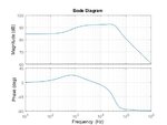
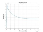
Now I use Matlab to plot this, for PSFB with the characteristics in the Matlab script below. You can see the bode and step responses for this transfer function with the attached images.

The problem is that I totally don't know what it should look like, neither if it's right or wrong and I don't have any power converter simulator here to check the bode response.

Is my approach good for solve this problem ? What do you think about these results ? What are your favourite power converter software simulators ?
Thank you for your help")
I am new on this forum. I have seen very interesting content here. I am a French student in electronic engineering in an apprenticeship program, so I also work in a company. And this year, my project is to design a 48V->350V 1kW Phase Shift Full Bridge converter. It's a fascinating project but this king of powerful converter is not the speciality here, so I would need your help for some details.
My converter is already fully designed and now I try to design the control loop. I would like to choose a current mode control to avoid the heavy capacitors, transformer flux imbalance and to allow an inherent current limiting. The only disadvantage I can see in this kind of control is the modelling part and I would need your help for this.
I read the Ridley's thesis about current mode control, I understand very well how it works, I have successfully applied it to buck converters but now I am stuck to do the same with my PSFB. I would like to get a model :
\[ \frac{i_{out}}{v_c} \]
With this, I will be able to use all the theory we know to design the outer voltage loop. I cannot find any model for a PSFB in current mode control so it seems I have to develop it by myself. For this, I have taken the Ridley's model :
In a first time, in order to design the control loop, I don't care about the feedforward terms, and I think it's the right things to do when I read the magazine from Ridley (Designers's Series - Part V - Current Mode control Modeling). So :
\[ G_{ic} = \frac{i_L}{v_c} = \frac{F_m G_{id}(p)}{1 + F_m R_i H_e(p)G_{id}(p)} \]
Now I use Matlab to plot this, for PSFB with the characteristics in the Matlab script below. You can see the bode and step responses for this transfer function with the attached images.
Code:
close all

Vin = 600;
fs = 100000;
Ts = 1/fs;
Vout = 360;
Rload = 70;
Ri = 4.2/200;
C = 5e-6;
L = 315e-6;
Llk = 52e-6; %inductance de fuite
N=1; %turns ratio Ns/Np
Rd = 4*N^2 * Llk / Ts;
D = Vout/(N*Vin);


Gid = N*Vin/Rload * tf([Rload*C 1], [L*C (L/Rload + Rd*C)  (Rload+Rd)/Rload])


%slope compensation
Sf = Ri * Vout/L;
Sn = Ri * (Vin*N - Vout)/L;
Se = Sf;


%modulator
Fm = 1 /((Sn + Se)*Ts)


%High frequency behavior
mc = 1 + Se/Sn;
w_n = pi/Ts;
Qp  = 1 / (pi*(mc*(1-D) - 0.5))
Hf = tf(1, [(1/w_n)^2 (1/(w_n*Qp)) 1])


Gic = feedback(Gid*Fm, Ri*Hf);
% step(Gic);
bode(Gic);

grid on
grid minor
h = gcr;
setoptions(h, 'FreqUnits','Hz');
The problem is that I totally don't know what it should look like, neither if it's right or wrong and I don't have any power converter simulator here to check the bode response.
Is my approach good for solve this problem ? What do you think about these results ? What are your favourite power converter software simulators ?
Thank you for your help