Continue to Site

Welcome to EDAboard.com

Welcome to our site! EDAboard.com is an international Electronics Discussion Forum focused on EDA software, circuits, schematics, books, theory, papers, asic, pld, 8051, DSP, Network, RF, Analog Design, PCB, Service Manuals... and a whole lot more! To participate you need to register. Registration is free. Click here to register now.

Compensation of LDO across corners

melkord

Full Member level 3
Joined
May 18, 2018
Messages
151
Helped
0
Reputation
0
Reaction score
1
Trophy points
18
Activity points
1,767
Hello,
I am trying to compensate an LDO across all corners.
My boss suggested me that I need to find a correct value for R3 and C3.
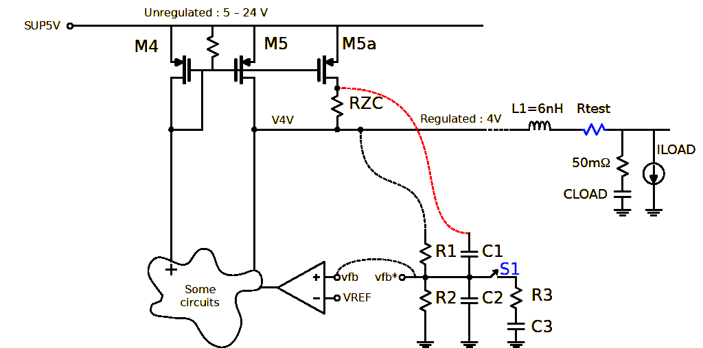
The picture below is the block diagram of the LDO.
My questions:
1. is there a way to find a correct value of R3 and C3 other than trial and error? so far, there are always corners whose PM is still below the spec.
2. I plot the transfer function of vfb*/V4V with different CLOAD when vfb is disconnected from vfb*. I was expecting CLOAD does not effect this transfer function, but it turns out, it does. Any explanation for it?

Thank you.
ldo.png
 
Show your results that are beyond expected load regulation errors due to ~Zo/Zload X 100%

R3C3 = T3 is a partial Ki gain pole
R2/(R2+R1) =Kp which controls Vout
Kd is the derivative gain compensation
Look up PID calibration methods.

Cload*ESR is another pole dependent on your loop gain for error reduction that is affected by your Zout. If it is low enough with high gain NFB then load regulation will be 1% at rated load. This also slightly affects s21 transfer function.
 
Last edited:
The biggest hassle I've had in LDO tweaking is the light load
where the pass FET is weak and soggy. At zero load you have
only the feedback shunt load and a really low frequency pole
if you've hung enough bulk C on the output to get decent step
response deflection.

Depending on how harsh your ground current spec is, you
might find a Class B or AB output (putting a sink device on
it) fixes light load dynamics.

Alternatively making other compensation elements follow
sensed load current and/or headroom (another loop issue,
low headroom removes most of the pass FET stage-gain
while high headroom light load makes it huge, how you
gonna straddle?) could flatten things out. But I don't have
any good, finer details to offer besides "try it and see".
 
Open Drain LDO’s vary RdsOn with load and NFB gain lowers that Rout.

BJT LDO’s use Darlingtons with fixed bias and so Rout is constant with NFB gain also reduces Rout.

Because of these differences, FET LDO’s will vary their Bode Plots with load and are more sensitive to Cout and ESR.
 

LaTeX Commands Quick-Menu:

Part and Inventory Search

Welcome to EDABoard.com

Sponsor

Back
Top