bart_ic
Newbie level 2

- Joined
- Sep 15, 2012
- Messages
- 2
- Helped
- 0
- Reputation
- 0
- Reaction score
- 0
- Trophy points
- 1,281
- Activity points
- 1,298
Hello Guys,
Firstly, I am new here, so please be forgiving to me
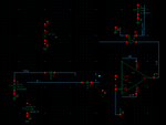
I am trying to design a comparator for CMOS image sensor ADC. Below you can see schematic of the testbench and waveform with results. Architecture of comparator, it is standard 2-stage opamp with high gain, without hysteresis. Operation of this circuitry should be like this:
On the begining, auto-zeroing of comparator is done by shorting the switch and rising Vpix to about 2V (reset level of pixel), same voltage appears on 'N' and 'P' nodes (Vramp is kept on 2.2V DC). Nextly switch is opened and Vpix is falling down to about 800mV. In this moment, voltages should look as follow:
Vramp=2.2V
Vpix=Vp=800mV
Vn=2V
Vout=0V
Final step:
Vramp begins to fall, so do Vn. When Vn equals Vp, comparator changes output state. Issue which I am observing is when Vramp begins to fall. In the same time Vp is falling to.... and I really do not know why. I will be very greatfull if anyone could help me with this problem

