Continue to Site

Welcome to EDAboard.com

Welcome to our site! EDAboard.com is an international Electronics Discussion Forum focused on EDA software, circuits, schematics, books, theory, papers, asic, pld, 8051, DSP, Network, RF, Analog Design, PCB, Service Manuals... and a whole lot more! To participate you need to register. Registration is free. Click here to register now.

colpitts oscilator questions

akbarza

Full Member level 2
Joined
Dec 18, 2013
Messages
131
Helped
0
Reputation
0
Reaction score
0
Trophy points
1,296
Activity points
2,556
hi
schematic:
1.png

I have written about this schematic in https://groups.io/g/LTspice/topic/102947920#150070 , and I take some explanation from that ltspice group members, but I want to know more explanation about it.
note: the schematic and .asc file is related to ltspice(I run it in ltspice)
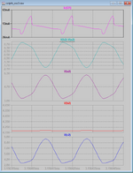
I uploaded a file as colpits_osc3.zip that contains colpits_osc3.asc and colpits_osc3.plt and a pic of this plt file.
as I know for a bjt transistor when v_be is approximately larger than 0.6 then the transistor is on and there will be a current from collector to emitter and if v_be<0.6( approximately) then it is off and there is no current from collector to emitter.
but as you can see in the plt file or its pic, for v(b2)-v(e2)<0.6 there is current, and also the pick of current occurred in v(b2)-v(e2)<0.6.
is it true?plz, explain
can explain to me about positive feedback that is needed for oscillation in this circuit.
if i delete c3, the circuit oscilate?
can explain to me, how the value of capacitors and resistors were chosen?
thanks
 
Hi,

first things first:
What do expect the circuit to do? Obviously oscillate. But at which frequency?

Then you talk about the transitor to be ON and OFF. But in this circuit I doubt the bjt is meant to be completely ON/OFF. I rather think it generatees some distorted sine shape. So continously current flow through collector, but continously rising and falling --> oscillating.

You talk about V_B2, V_E2, I_C2 ... but you don´t give values. Please show the simulation results.

For my taste the inductance is very low, it needs a very high speed current rise to generate a useful voltage across the inductance.

Klaus
 
Each oscillator circuit that is intended to produce a sinus-like signal requires
(a) an amplifier working in the quasi-linear operating range and
(b) a positive feedback path which allows unity loop gain for one single frequency only.

These requirements can be fulfilled by the shown circuit.

* The transistor works in common base configuration with zero phase shift between input (emitter) and output (collector).

* The feedback path between collector and emitter consists of a tank circuit (L is signal grounded via V1 in parallel to the series connection C1-C2).
This parallel resonant circuit produces zero phase shift at the resonant frequency wo.
A part of the voltage developped across the tank circuit is fed back to the emitter - thus providing positive feedback at w=wo.
 
The finer details of Colpitts, Clapp and other Sinewave BJT Oscillators
  • Here I compare two methods of LC sine oscillators with 1 inductor.
  • The ideal 50% of max amplitude is partially regulated by Vbe nonlinear pulse load so Vo is not a regulated amplitude (no AGC).
  • Beware of negative effects on hFE, Vcc noise and load resistance in each case below.
  • The base resistance controls current and voltage gain as well as Zc/Ze impedance ratio.
  • The most stable clean sine wave is when gain is just slightly greater than unity (1) and Vo is roughly 50% (undistorted) of max Vpp swing (distorted).
  • In both cases the oscillator is basically a pulse of base current then it resonates with high Q. so distortion must be regulated by carefully controlling loop gain just enough to sustain oscillation plus 10% or so for tolerances. Too much gain will cause saturation effects on one half of the sine wave peak.
  • The gain also refers to the level of the Ib base current pulse relative to the sine current. (see scope simulation from Falstad site)
  • Both are hFE sensitive but since these oscillators are pinged by pulses to Vbe, they are suitable for high GBW transistors with very low hFE (e.g. = 10)
  • To scale frequency 1st choose an impedance value for 1/sqrt(LC)*f*2pi, this examples X(f)~ 1kohm then choose each L,C value.

1. Positive Feedback (+FB) method uses a smaller cap say 10% of C1 resonant cap to emitter to boost amplitude in phase.
  • Inductor L on Vcc permits a double max amplitude distorted output at Vcc+/- Vcc.
  • But since it has higher || Q it is much higher output impedance, but also better supply noise immunity. the emitter is biased to only produce pulse current at low duty cycles on peak then float open circuit.
  • This is a common base (CB) amp with the Vb at constant voltage and Ve modulated by the tiny pulse per cycle from negative peak of Vc (out), which pulses Vbe to inject current for L||C to ring with high Q.

2. Negative Feedback (-FB or NFB) method uses two caps of equal value thus equivalent resonant C is C/2 or the equivalent value if mismatched, but optimal performance is usually matched.

This is a common emitter (CE) amp with DC gain Rc/Re but AC gain boost by Re bypass cap. Then Rfb feedback improves sine quality, lowers output impedance and controls attenuated of NFB to get gain just slightly greater than unity. Unfortunately, all Vcc noise is passed to output, reduced slightly by the amount of NFB. But the clear advantage is a much lower output impedance = Rc so the load will affect output amplitude but not the Q of the resonator buffered by the transistor gain from base resonance signal.

1701982911692.png

Since the CE amp increases gain with hFE, using NFB means more fedback signal and thus reduces the output level.

Normally one chooses the next stage impedance much greater (e.g. 10x) than the output impedance of these amplifiers and AC couples if DC offset must be removed.
Here is my comparison simulation for 3.3V. To use a large supply all R values are typically scaled up and keep similar ratios.

These are fundamentals and not the optimal design found in more complex designs used in signal generators, but they are simple.
 
Last edited:
Hi,

first things first:
What do expect the circuit to do? Obviously oscillate. But at which frequency?

Then you talk about the transitor to be ON and OFF. But in this circuit I doubt the bjt is meant to be completely ON/OFF. I rather think it generatees some distorted sine shape. So continously current flow through collector, but continously rising and falling --> oscillating.

You talk about V_B2, V_E2, I_C2 ... but you don´t give values. Please show the simulation results.

For my taste the inductance is very low, it needs a very high speed current rise to generate a useful voltage across the inductance.

Klaus
I tried to upload the result of the simulation when I began this threat, but I could not. below pic is the result of the simulation(I tried three times to upload it successfully).
also, the circuit simulation shows an oscillation. the below pic is a very small part of the simulation.
 

Attachments

  • Colpitts_osc3.PNG
    Colpitts_osc3.PNG
    29 KB · Views: 44
I tried to upload the result of the simulation when I began this threat, but I could not. below pic is the result of the simulation(I tried three times to upload it successfully).
also, the circuit simulation shows an oscillation. the below pic is a very small part of the simulation.
What now is the problem?
Question: In your 1st picture the supply voltage is 6V.
In the simulation I see a maximum of app. 9 volts. What is your explanation?
 
Hi,

first things first:
What do expect the circuit to do? Obviously oscillate. But at which frequency?
No answer?

***
So what are you worried about?
The current of IC (Q1) vs V_BE?

There are several specifications in the datasheet. (Sadly you did not post a link. Thus I used the ON Semiconductor one. )
Do you understand the specifications:
* Output capacitance
* Input capacitance
* Delay time
* Rise time
* Storage time
* Fall time
.. and what this means in a circuit?

Klaus
 
What part did you not understand in my answer?

- adjust Rb to get Vo to be approximately 50% of Vcc
--- Updated ---

Hi,


No answer?

***
So what are you worried about?
The current of IC (Q1) vs V_BE?

There are several specifications in the datasheet. (Sadly you did not post a link. Thus I used the ON Semiconductor one. )
Do you understand the specifications:
* Output capacitance
* Input capacitance
* Delay time
* Rise time
* Storage time
* Fall time
.. and what this means in a circuit?

Klaus
I believe that none of this relevant.

Only the Ic = gm * Vbe exponential characteristic pulse shaped by the very narrow current pulse by the methods I described previously.


1702051091545.png
 
Last edited:
i
Hi,


No answer?

***
So what are you worried about?
The current of IC (Q1) vs V_BE?

There are several specifications in the datasheet. (Sadly you did not post a link. Thus I used the ON Semiconductor one. )
Do you understand the specifications:
* Output capacitance
* Input capacitance
* Delay time
* Rise time
* Storage time
* Fall time
.. and what this means in a circuit?

Klaus
I think a bjt has current when vbe is larger than 0.6-0.7, but in this simulation, I saw that when vbe<0.6, there is current from collector to emitter. I want anyone to clear this with me and explain why there is a current when vbe<0.6.
--- Updated ---

The finer details of Colpitts, Clapp and other Sinewave BJT Oscillators
  • Here I compare two methods of LC sine oscillators with 1 inductor.
  • The ideal 50% of max amplitude is partially regulated by Vbe nonlinear pulse load so Vo is not a regulated amplitude (no AGC).
  • Beware of negative effects on hFE, Vcc noise and load resistance in each case below.
  • The base resistance controls current and voltage gain as well as Zc/Ze impedance ratio.
  • The most stable clean sine wave is when gain is just slightly greater than unity (1) and Vo is roughly 50% (undistorted) of max Vpp swing (distorted).
  • In both cases the oscillator is basically a pulse of base current then it resonates with high Q. so distortion must be regulated by carefully controlling loop gain just enough to sustain oscillation plus 10% or so for tolerances. Too much gain will cause saturation effects on one half of the sine wave peak.
  • The gain also refers to the level of the Ib base current pulse relative to the sine current. (see scope simulation from Falstad site)
  • Both are hFE sensitive but since these oscillators are pinged by pulses to Vbe, they are suitable for high GBW transistors with very low hFE (e.g. = 10)
  • To scale frequency 1st choose an impedance value for 1/sqrt(LC)*f*2pi, this examples X(f)~ 1kohm then choose each L,C value.

1. Positive Feedback (+FB) method uses a smaller cap say 10% of C1 resonant cap to emitter to boost amplitude in phase.
  • Inductor L on Vcc permits a double max amplitude distorted output at Vcc+/- Vcc.
  • But since it has higher || Q it is much higher output impedance, but also better supply noise immunity. the emitter is biased to only produce pulse current at low duty cycles on peak then float open circuit.
  • This is a common base (CB) amp with the Vb at constant voltage and Ve modulated by the tiny pulse per cycle from negative peak of Vc (out), which pulses Vbe to inject current for L||C to ring with high Q.

2. Negative Feedback (-FB or NFB) method uses two caps of equal value thus equivalent resonant C is C/2 or the equivalent value if mismatched, but optimal performance is usually matched.

This is a common emitter (CE) amp with DC gain Rc/Re but AC gain boost by Re bypass cap. Then Rfb feedback improves sine quality, lowers output impedance and controls attenuated of NFB to get gain just slightly greater than unity. Unfortunately, all Vcc noise is passed to output, reduced slightly by the amount of NFB. But the clear advantage is a much lower output impedance = Rc so the load will affect output amplitude but not the Q of the resonator buffered by the transistor gain from base resonance signal.

View attachment 186743
Since the CE amp increases gain with hFE, using NFB means more fedback signal and thus reduces the output level.

Normally one chooses the next stage impedance much greater (e.g. 10x) than the output impedance of these amplifiers and AC couples if DC offset must be removed.
Here is my comparison simulation for 3.3V. To use a large supply all R values are typically scaled up and keep similar ratios.

These are fundamentals and not the optimal design found in more complex designs used in signal generators, but they are simple.
hi, thanks for your reply
please tell me if this statement is true or not:
There is positive feedback from the emitter to the collector and there is negative feedback from base to collector. if positive feedback gain in a frequency is larger than negative feedback gain in the same frequency, then there is an oscillation in that frequency.
 
Last edited:
I guess ... if I asked a third time ... it would not make you answer my queastions.
So I better don´t waste our both time.

Klaus
 
I guess ... if I asked a third time ... it would not make you answer my queastions.
So I better don´t waste our both time.

Klaus
hi
in a bjt, if vbe<0.6 then is it possible that there is Ic? If your answer is positive in which condition? For example, if vbc is forward and vbe<0.6, is it possible that there is ic?
 
hi
in a bjt, if vbe<0.6 then is it possible that there is Ic? If your answer is positive in which condition? For example, if vbc is forward and vbe<0.6, is it possible that there is ic?
Current is exponential with Vbe so there is current continuously even at Vbe =0.5 but to make with work follow my design rules and see how Vbe is almost constant at 630 mV with a pulse that double the sine base current from 80 uA pk to 160 uA with the pulse to excite resonance.

There is no negative feedback in yours and mine on the right and only 10 pF or more is needed to advance the phase of positive feedback then the Barkhausen criteria is satisfied. You need to follow my description and understand how to bias the input to have just enough Vbe to produce 40 to 70% of max swing to have a clean stable sine wave. Too little it stops oscillating. Too much and the pulse tries to saturate Vce and distort the sine.
--- Updated ---

Added Ib min to plot on bottom
http://www.falstad.com/circuit/circuitjs.html?ctz=CQAgbALCCMB0CsAGZLWoEwFMC0AOEisAzOtNOgOyLwRHTxHxj0wjxuJs5kBQANjAhRy+dOmHp8nQinpp5skNhnIiATngaUFCImZhcYAjwDGIMRNHjz1zkWLdpsXLohqxYOmDWGiUFdA8AC7mTDCSIESIlgSs2HAu6GCIRCQuuEQUYBREBLCQ0BTuFEXw6GXi6OHsACaYAGYAhgCufEGmgjHQQjb+kQ7xnHCMlBQuyGBluFlVATwA7pHRIGpGUcLkxovdUBa9+4gL+yKhRieHi3tXYXsXnStnPec8AE73q-sfnAbIR3sf6wexgA5ktdtZAeJpMYAPKRMowTa0KpkWbGAAeiIoME8MEyOKMwiMAGFApjoGpctAwFVSFTJiAiSBiehXmDGfhAV8YL83oCduzbpEiH8bhDlrceAAHeFVCCchGoyKMrbgXT7ZJWfwdKb7XXncywdAKBREHBqJToWApY2GNw09BqZAQIxzMyQIY9D1AobcaBKeyUaCZZiURB0xh5ZCBRbZKofb1faUgKhQeUp5YAlV3XV7eBZA5s-OPKDFg7Cw5vTV6gtClSyHiY5jsY25TycY2E8LMkVNzaQcCO8DY4RQUk8OGpoFjKDcw6gst52thaQ8ABK7PT5UJUli6vsuWhhHgRYi6f1ESGSF+ixGiKq-M2OYLAu9ApzZ-wZfTz6MCcQ+BJosZYfGWSqHO66rpomrowAgjhKMMFByIw8C4NuKQuFGiCBCEF5fi+l5xFanhqBAhR6MaYapK6+R0BoTqQGoZFRP6SAgHUTStO0kGelA3pCtA5pwboOGULQ5BEN4OjsHMAjfgRf6wfWcgmmg-oqGUYzUNkECaPA1KXkcClqpwP5HHG06Zq6Fnqv+gE2U2AHhPx6BUpQKqbCyPC6LkNEwAWLq7OqQzoAA+tAYWIBFURgGAYVWrgei4KsJQQDoQh0LgUXWtGYXxBFPkpOAuD4CcuDUuYIXmGoEVRTFejxfA1okFkqQGd0GQkDlsj5ZFZIcmc2JZKIZkgPgAA6UoAGIAEITQAzjCC0mAAlnwfCNEEAD2LwADSLQAatti0ALaNOii0TQAjot6AAFSHSYJiLQARs0QSLQAMttjQ1ItAB8N3QMgADWB0Le9n2Q5gQRBJgLxHc9i0AHbbatC2YItq2nadzQo6tQQAJ6Nni2KVUQ6EwBaUD4NgABuWMLXNi3bSt62bTt+2LXw23zKzH1Sh92OnVKmA1I0KMmJgENQ4tUrbbtSMvQtaMY0zON4wTxOwOubCfhyZm7mZdjELETgnuSBmIfgbWIewEggAAKvMJ0LadsMABbbTUC2s-Ui3QAAsgAEgAXotC2rSjTPLSYsCLQACi8bNXY0i3EttKN+wtACSdSNHwR3bcLUc5wAAotSAAKTFwAFAtW0AJRnRdi31ErK18JgkuR9HTO89tUqLcCjTR5HfCrcCntBHwRNAwt0AQ6T5BrHKbjwiq+AANKYJgw8LWuJgAPRrkzAB+RCLZL-2NzUABWzQLdDa71K97ed4PB+j+Pz9u40JhParUwIzI6UoD7nyrogauT0VYZ2gNjFGkcEbAJzvMQmnsM6skxEITkVRphrAduNZkCCFrH2Pt9D+iMFodwhiyAAPPQ+B18UZE0WvTQuzQmYd2oVNOadCr4LSBtdEGl0FqkkWjtN6itn6szFkghaX8R5jxRgAbmLotOoJgXg90xmgjBi0gHTwRoY6aABRduKdTpXRmrNUmkxsTYHUCmKgAYuz4CdlnNhC0ADK8N5iNBeNDMxZiADkFB4CLQoNgAAIpgEw2AqIim2pEC0-p0nlHSthHC2SyDdCYEgIoLp4BIAyLEQIQA
 
why there is a current when vbe<0.6.
Common-base mode operates the transistor by increasing or reducing voltage of the emitter leg instead of changing bias at the bias terminal. It's just another method of changing the b-e relationship, in order to alter the transistor's conduction.

It's what makes common-base operation different from common-emitter or common-collector. Common-base mode is useful when the signal is low impedance. A chart of the different operating modes compares the different characteristics.
--- Updated ---

See discussion (with helpful diagrams):

electronics.stackexchange.com/questions/172451/confusion-with-transistor-modes
 
Last edited:
Correction 82uA to 111 uA from right OSC Base current sine to pulse pk. Closer levels means less distortion.

In this common base case the tiny 10 pF positive feedback is only low impedance for narrow pulses, hence why LC Colpitt’s Oscillators tend to be pulse driven.
 

LaTeX Commands Quick-Menu:

Similar threads

Part and Inventory Search

Welcome to EDABoard.com

Sponsor

Back
Top