Continue to Site

Welcome to EDAboard.com

Welcome to our site! EDAboard.com is an international Electronics Discussion Forum focused on EDA software, circuits, schematics, books, theory, papers, asic, pld, 8051, DSP, Network, RF, Analog Design, PCB, Service Manuals... and a whole lot more! To participate you need to register. Registration is free. Click here to register now.

collector coupled transistor monostable circuit

Status
Not open for further replies.

avskalai

Newbie level 6
Joined
Jul 15, 2011
Messages
11
Helped
0
Reputation
0
Reaction score
0
Trophy points
1,281
Activity points
1,386
By referring to the values below, I am trying to design a positive edge triggered collector-coupled monostable multi-vibrator using two n-p-n transistors. The circuit is attached below. Please guide me on the necessary calculations needed to make the circuit to work. I need the circuit to produce a pulse of about 1.5ms upon trigger. I did my own calculation. Please correct me if I am wrong. Thanks in advance.


BC237B
Values from datasheet.
VCE (sat) = 0.6V
VBE(sat) = 1.2 V
IC (max)? ?100 mA
HFE (min) =200

BC327B
Values from datasheet.
VCE (sat) = 0.7V
VBE(sat) = 1.2 V
IC (max)? ?500 mA
HFE (min) =160


i) Rc = V cc- V ce (sat) / Ic (sat)

= 12V-0.6V/ 50mA
˜ 220?

ii) RB2 = V cc- V be(sat) / IB2


iii) IB2(min) = Ic (sat) / h FE(min)

= 50mA/200 = 0.25mA


So in order to saturate Q1, the base current supplied will be 5 x IB2(min)

IB2 = 5 x 0.25mA=1.25mA

So, R1 will be = V cc- V be(sat) / 1.25mA = 12V-1.2V / 1.25mA = 8640?


I choosed the nearest value resistor = 10k?

T = 0.69RC

So C = 1.5ms / 0.69x10K ˜ 220nF


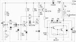
I need guidance for the next step, that is to calculate the values of R2 and R3. Q1 must be in cut off and only be switched on by a positive edge signal. And also I need an explanation regarding the example circuit below. I need to trigger my circuit in the same way as the example circuit below.

1) What is the purpose of R1, C2, D1,D2 , D3 and D4 ?
: From what I had studied, is that C2 forms a capacitive coupling to prevent the DC voltage from flowing to base of Q1, but allows an AC signal to pass through. By using a simulation software, I observed that there is a voltage spike on the base of Q1 every time the switch is opened.
Diode D2 allows the negative spike to flow through ground preventing the negative spike to flow to the base of Q1.

Am I right? Please correct me if there is a mistake.

Please explain to me how a voltage spike on the base of Q1 turns the transistor on. The spike value on the scope trace is about +2V.


2) Why the voltage value on the base of Q1 is negative in value.
I had set the resistors value based on the example circuit and noticed the voltage on the base of Q1 is negative.


3) Resistor RA and RB forms a voltage divider used to bias Q3.
Am I right?

How to calculate the values for RA and RB based on my first circuit which uses 220? resistor as RC?


Expecting some detailed explanations or simply a link for better tutorial or theory/books for better understanding of the transistor circuit theory. ThANKS IN ADVANCE.
 

Attachments

  • circuit 1.bmp
    88.8 KB · Views: 103
  • example circuit.jpeg
    example circuit.jpeg
    40.7 KB · Views: 278

I think you know that the connections on your circuit are not all like the original ones.

I didn't mean the component values.

Added:
If you like to discuss your circuit in details. please try to give for each component a specific reference... I see 2 Rc, for example.
Oh... it seems only these 2 Rc have the same reference :smile:

So the first step is: let us find the wrong connection(s) in your circuit ;-)

Meanwhile...
i) Rc = V cc- V ce (sat) / Ic (sat)
= 12V-0.6V/ 50mA
˜ 220?

How did you get the... 50mA ?
Don't worry we will talk about this when you will correct your the schematic of your circuit (don't forget the Rc's :) )
 
Last edited:

Re: collector coupled transistor monostable circuit

I think you know that the connections on your circuit are not all like the original ones.

I didn't mean the component values.

Added:
If you like to discuss your circuit in details. please try to give for each component a specific reference... I see 2 Rc, for example


Thanks for your reply. The first circuit named "circuit 1" is a part of the "example circuit".
I am trying to split the circuit into 2 blocks by 1) separating the input trigger signal section and 2) monostable multivibrator circuit. The problem is in the monostable section because the original author of the "example circuit" put up a remark note not to build the circuit because there are some corrections that need to made in order for proper operation. I am trying to design my own collector coupled transistor monostable circuit. The 2 Rc are of the same value. 220Ω on both transistors collector. Now the question is the biasing of transistor Q1?
Expecting a reply... Thanks
 

I meant there is something wrong in your part ... the split is wrong... It is like a puzzle ... not easy to detect :)
If you don't have time to find it... I will be pleased to show it for you :grin:
 

The maximum collector current that can flow safely in both transistors according to the datasheet are 100mA. I set the collector current at 50mA. Anyhow, Q2 is saturated?
 

I think if we will keep discussing your circuit... I hope I will be able to help you on how to calculate things when using transistors... in a simple and right way.

Added:
A hint about the wrong connection... how Q2 will be able to drive Q3?
I assumed Q3 is important to you since you asked about RA and RB... and it is Q3 which will give the negative pulse if connected properly.
Please don't hesitate to ask for another hint ;-)

Try to complete the connections for RA and RB... I think your circuit will be correct and ready to be analyzed (with Rc1 and Rc2 :smile: )

I am sorry... I have the habit not to jump over any mistake (since I use to make many silly mistakes every time I design a circuit).

Good... I think you are adjusting your circuit (I mean the part of interest).
Please don't forget to add the load (a resistor Rc3 for example) between the collector of Q3 and ground... I hope you have an idea of its value because it will be the start to calculate the component values for the rest of the circuit.

Even if you are no more interested, I like to point out that the 4 components you omitted at the circuit input (R1, R2, D1 and C1 in the original one) are important for the proper functioning of the monostable. So to design correctly the input part, one must know in advance the kind of the source that will geneate the input signal and its strength (voltage and current) assuming it is squarewave. In the original circuit, the driver is a mechanical on/off switch.

Good luck

Kerim
 

Attachments

  • NegTrig_02.png
    NegTrig_02.png
    130.8 KB · Views: 125
Last edited:

Attached is a new schematic diagram. I need guide to calculate the biasing resistor R2 and R3 AND RA, RB.

*Kerim "Even if you are no more interested, I like to point out that the 4 components you omitted at the circuit input (R1, R2, D1 and C1 in the original one) are important for the proper functioning of the monostable"

Please explain with more details. ThanksClip.jpg
 
Last edited:

Ok... First I like to point out that I attached yesterday a schematic (comp_02.png to post #6) but I don't see it every time I open this thread so I wonder if it happened to you to see it once.

Now let us explore your circuit.
I am analyzing your output... it is supposed to get a spark I guess.
Do you know that the collector breakdown voltage of TIP142 is only 100V while in the original circuit is 400V. Is this ok to you?
I will not wait your answer(s)... I will go on anyway.

In any case there will be a need to add one or more zeners at the collector of the power transistor (darlington) Q4.
The zener voltage (of the sum if more than one) should be less than its breakdown voltage.
It is important that the output pulse voltage (its peak) is suitable to drive the primary coil of the output transformer to get the expected spark.
You omitted the resistor between the Q4 base and ground. This resistor helps usually in increasing the Vce breakdown voltage and in speeding up the transistor turn off.
Now the missing value is the DC resistance of the primary coil which determines the DC current at the Q4 collector when on. Do you have an idea about it? In the original circuit it is about 1.6 Ohm.
To get the same spark power, if the primary voltage is reduce, it DC current should be made higher (by having a lower resistance).
If Rcoil=1.6 Ohm, the collector current of Q4 will be (typically) :
Ic = Icoil = (Vcc - Vsat)/Rcoil = (12 - 2)/1.6 = 6.25 A

Let us assume, as an example, that we will use TIP142 with a transform DC resistance of 1.6 Ohm hence Ic4 = 6.25 A
Before I forget, two power zeners (BZX85C47 or equivalent) should be added between Q4 collector and base. The collector peak voltage (while the primary is discharging) will be:
Vc4_peak = 2*Vz + Vbe = 47V + 47V + 2 = 96 V
Actually the values of Vz and Vbe might be a bit higher due to the relatively high feedback current.
Using more than one zener to get a required voltage drop, lets the pulsed current generate lower instantaneous power in each zener (P=Vz*I).

It is time to calculate the Q4 base current:
Typically to get a practical low Vsat for darlingtons we drive the base with a current Ib so that:
Ic/Ib is the range between 100 to 500
Ic is detrmined by the load and Vcc. By negleting Vsat Ic = Vcc / Rload (actually it will be lower since Vsat is small but not zero).
In this circuit we will assume Ic/Ib for Q4 is equal to 200:
Ib4 = Ic4 / 200 = 6250mA / 200 = 31.25 mA
Therefore:
Ic3 = Ib4 + Irb4
Rb4 is of the (omitted) resistor between base and ground.
Rb4 = Vbe4 / Irb4
Also practically we choose Ib/Irb to be equal in the range 3 to 10 (or higher, in any case one should consider other factors if the application is critical). Here we will choose:
Ib4/Irb4 = 5 , and assuming Vbe4 is about 2V, this gives:
Rb4 = Vbe4 / Ib4 * 5 = 2 / 32.25 * 5 = 0.32 Kohm
Rb4 = 330 Ohm (standard value)

Continued on post #10.
 
Last edited:

Yes, I know the collector breakdown voltage of TIP142 is 100v. This is not my primary concern. In my test board, I am using a 400V rated 15A darlington transistor with zener clamping diode between the base and the collector.The transistor is BU941. Any how, the reason I posted the circuit is to complete the monostable section ( block 2) of the circuit. Once I can get that working properly, I am able to do the remaining circuit myself.

For calculation purpose, lets assume that the Q4 collector current is limited by the resistance of the primary side of the ignition coil since Q4 is used primarily as a switch. What is missing is the value needed to drive base of Q3 which will saturate the transistor Q3 which in turn switch on Q4. The base resistor of Q4 should supply enough base current to drive the transistor into saturation. Assume Ic of Q4 is 10A. Minimum base current= Ic(sat)/hFE:
= 10/300(values from datasheet) = 33mA. Lets give the base current 5xmin base current= 150ma to ensure saturation.

Rb of Q4 should be : Vcc-Vce(sat)/Ib= 12-2/150mA= 66ohm. So RC3 should be 50 ohm. Done. Now, I need help on the monostable section of the circuit. I need help on that part.
 

Should I restart the calculations for Ic4 = 10 A instead of 6.25 A ?

Anyway I will go on.
It is time to calculate Rc3:
Rc3 = (Vcc - Vsat3 - Vbe4)/ (Ib4 + Irb4)
where:
Vcc= 12, Vsat3=0.4V , Vbe4=2V, Ib4=31.25mA and Irb4=Vbe4/Rb4=2/0.33= 6mA
Rc3 = (12 - 0.4 - 2) / (31.25 + 6) = 0.258
Rc3 = 220 Ohm
In this case:
Ic3 = (Vcc - Vast3 - Vbe4) / Rc3 = (12 - 0.4 - 2) / 0.22 = 43.6 mA

By the way, you will be able to check the validity of the figures I am giving you when you will build the circuit and take measurements on it. Obviously since the start given data (Ic4 = 6.25 A) may not be the real one on your circuit there will be differences in all other values. For instance, changing Ic4 from 6.25 A to 10 A (hence much closer to the current limit of Q4) some chosen constants (said practical) should be changed accordingly.

It is time to calculate Ib3.
Typically to get a practical low Vsat for BJT transistors we drive the base with a current Ib so that:
Ic/Ib is the range between 10 to 25
Here Ic3/Ib3 = 20 is good to get Vsat3 = 0.4V for Ic3= 43.6 mA (actually it will be lower).
Ib3 = 43.6 / 20 = 2.18 mA
Now Rb3 = RA = Vbe3 / Ira
Here, Ib3 / Ira can be assumed 10 (even higher but it seems to me you like the high currents ;-) )
Vbe3 = 0.75V
RA = Vbe3 / Ib3 * 10 = 0.75 / 2.18mA *10 = 3.44 Kohm
RA = 3.3 Kohm

What is about RB?
RB = (Vcc - Vbe3 - Vsat2 - Vdiode) / (Ib3 + Vbe3/RA)
where
Vsat2 = 0.25V and Vdiode = 0.7V , Vbe3/RA= 0.75/3.3 = 0.23 mA
RB = (12 - 0.75 - 0.25 - 0.7) / (2.18 + 0.23) = 4.274 Kohm
RB = 3.9 Kohm

I remember you asked about the function of D4 and D2.
Let us see D4 first:
When Q1 is off, C2 will be charged by Rc1 through Vbe2 and D4. Its voltage will be:
Vshg = Vcc - Vbe2 - Vd4 = 12 - 0.7 - 0.7 = 10.6 V
When Q2 is turned on, Vc1 becomes close to 0V (actually close to Vsat1 + Vd2).
The other terminal of C2 at the base of Q2 drops at the same time to -10.6V
Typically, the reverse base0emitter breakdown voltage is not high, it is about a few volts. Adding D4 in series with emitter will prevent the -10V.6 to generate a realtively high reverse current. The reverse current will be determined by D4 which is rather a very low reverse current at -10V.

Continued on post #12
 
Last edited:

Thanks for showing the calculation involved. Perhaps I should have been more patient and solve one step at a time before the next . I am doing my calculations now. I have attached a new schematic with corrections. Please take a look and rectify any mistake. And the next step would be finding values for R2 and R3. And yes, I did asked about the function of D2, D3 and D4. Any explanation??99.jpg
 

The diode D2 is not really necessary in this circuit and can be omitted. The base-emitter junction is already protected from a possible reverse breakdown by D3.

It is time to calculate Rb2 which has two functions; to drive Q2 and to charge C2 hence determining the pulse time.
Ic2 = (Vcc - Vbe3 - Vsat2 - Vd4) / RB
Ic2 = (12 - 0.75 - 0.25 - 0.7 ) / 3.9
Ic2 = 2.63 mA

Let us assume Ic2/Ib2 = 20
Ib2 = 2.64 / 20 = 0.132 mA

The maximum value of Rb2 is therefore:
Rb2 = (Vcc - Vbe2 - Vd4) / Ib2
Rb2 = (12 - 0.7 - 0.7) / 0.132 = 80.3 Kohm

Before deciding on the final value of Rb2 (since it can be any value below 80K though not too very low), let us find out the formula related to this circuit that gives its pulse time.
First, I will assume that D2 is not removed.
The time is set mainly by C2 and Rb2.
As we saw earlier:
Vshg = (Vcc - Vbe2 - Vd4)
At the time Q1 is turned on the disharge (actuall reverse charge) circuit consists of:
Vcc, Rb2, C2, Vsat1 and Vd2

Continued on post #14
 
Last edited:

I will let you finish the step and then I will ask any questions if I don't understand.

The time constant is T= 0.69RC.
 

The time constant is T= 0.693*RC.

This is true in a special case when Vc(t) = 1/2 Vtotal (assuming Vc(0) = 0V)

Let us remember the general form of the capacitor (C) voltage while it is charged charged through a resistor R.

Vc(t) - Vc(0) = [ Vmax - Vc(0) ] * [ 1 - e^(-t/RC) ]

At time 0 we found that the voltage of C is -10.6 V
Vc(0) = -10.6

Vmax = Vcc - Vsat1 - Vd2

What is about Vc(t)?

Q2 will start to turn on again when:
Vb2 + Vd4 = Vc(t) + Vsat1 + Vd2
Vc(t) = Vb2 + Vd4 - Vsat1 - Vd2

Therefore the equation becomes:
Vb2 + Vd4 - Vsat1 - Vd2 - Vc(0) = [ Vcc - Vsat1 - Vd2 - Vc(0) ] * [ 1 - e^(-t/RC) ]
0.7 + 0.7 - 0.2 - 0.7 + 10.6 = [ 12 - 0.2 - 0.7 + 10.6 ] * [ 1 - e^(-t/RC) ]
11.1 = 21.7 * [ 1 - e^(-t/RC) ]
0.511 = [ 1 - e^(-t/RC) ]
This gives approximately t = 0.69 * RC as you said, since 0.511 is close to 0.5

Actually C2 could be chosen as 100n and Rb2 = 22K to produce 1.5 ms (approximately)

Now how Rc1 value can be determined? What is the function of Rc1 in this circuit?
Rc1 sets the recharging time of C2 to 10.6V when Q1 is off.
Could you find the time formula for which C2 is charged again to 95% of 10.6V?
Now t=0 is when Q1 is turned off (Q2 is on).

Vc(t) - Vc(0) = [ Vmax - Vc(0) ] * [ 1 - e^(-t/RC) ]

Vc(0) = - ( Vb2 + Vd4 - Vsat1 - Vd2 )
Vc(0) = - ( 0.7 + 0.7 - 0.2 - 0.7 )
Vc(0) = - 0.5 V
Note: Vc(0) = -Vc(t) of the previous calculation

Vmax = Vcc - Vbe2 - Vd4
Vmax = 12 - 0.7 - 0.7
Vmax = 10.6 V

Vc(t) = 0.95 * 10.6 = 10.07

10.07 + 0.5 = ( 10.6 + 0.5 ) * [ 1 - e^(-t/RC) ]
0.9522 = [ 1 - e^(-t/RC) ]
t = RC * ln [ 1 / ( 1 - 0.9522 ) ]
t = 3.04 * RC

Actually we can assume for a better recharging:
t = 10*RC
So if we know the minimum delay between the pulses:
Rc1 = Tmin/C2/10
Let us assume Tmin = 10ms
Rc1 = 0.01/100e-9/10
Rc1 = 10K

Note: This minimum delay time between two pulses should not be shorter than the time needed for the primary coil current to restore its expected maximum value (close to 6.25A in our example here).
Any comments or questions?
 
Last edited:
This is way too complicated;almost driving my brains into saturation.. I will take my time to go through your calculations. BTW, almost all textbook dont go this far to set the collector resistor of Q1. Most example circuit uses collector resistors with identical values. RC1=RC2. What do you mean by Tmin?
 

You may simply assume
t = k * RC
where 3 < k < 10 which depends on the application
Obviously k > 10 is not wrong but the capacitor is already well charged for 10RC.

About Tmin, the input signal should wait before sending another pulse so that the transformer is ready again to be pulsed.
If the input signal is made manually, the interval between pulses is always relatively long in comparison with 1.5 ms

Most example circuit uses collector resistors with identical values. RC1=RC2

I am afraid, as a design idea Rc1=Rc2 is wrong though it works but each resistor has a different function as we saw.

I think it becomes late where you are... if you like we will continue later.
 
Last edited:

Its ok with me. Thank for your time. If can, please show the remaining calculation needed to determine values of R2 and R3. If I am not mistaken, the maximum interval of two pulses is about 2ms. That is if a 4 cylinder car engine running at 6000 rpm. So is the 10K Rc1 suitable.
 

Oh... so the ignition transformer is also fast to recover its charged state.
For Tmin = 2ms
0.002 = 10 * 100e-9 * Rc1
Rc1= 2K , we can let it 1K (to have a margin)
So
Rc1 = 1K

Now we can calculate Ic1 :
Ic1 = (Vcc - Vsat1 - Vd2) / Rc1
Ic1 = (12 - 0.2 - 0.7) / 1
Ic1 = 11.1 mA

Ic1/Ib1 = 20 (as usual for small transistors for typical Ic currents; not too high or too low)
Ib1 = 11.1 / 20 = 0.555 mA
Instead of writing many equations with many variables and solve them, we assume one of the variables and continue sequentially.
For example we assume that the current in R3 is equal to Ib1. In other words, to turn on Q1, 2*Ib1 will be needed.

R3 = (Vbe1 + Vd2) / Ib1
R3 = (0.7 + 0.7) / 0.555 = 2.52 Kohm
R3 = 2.2 K (standard value)

For Q1 to stay on during the pulse even if the input pulse current is returned to zero (when C1 is fully charged), R2 should provide the Ib1 and Ir3 at the base of Q1.
This happens when Q2 is off, so the path of interest is:
Vcc, Vbe3, RB, R2, Vb1 to ground
The loop equation here is:
Vcc = Vbe3 + R2*[ Ib1 + (Vbe1 + Vd2) / R3 ] + (Vbe1 + Vd2)
R2 = ( Vcc - Vbe3 - Vbe1 - Vd2 ) / [ Ib1 + (Vbe1 + Vd2) / R3 ]
R2 = ( 12 - 0.7 - 0.7 - 0.7 ) / [ 0.555 + (0.7 + 0.7) / 2.2 ]
R2 = 8.3 Kohm
This is the maxium value for R2.
It is better to choose a lower value so that even Q2 is not fully off (hence Ic2 is not zero and there is a drop on RB) there is enough feedback current to keep Q1 on. About half of the calculated value is good. The value 3K9 or a bit higher as 4K7 is a good choice.
Uusally the designer adjust the best values during the final test. The values we calculate help to have a good start. while many of them will likely don't need to be changed, it is not a crime to adjust some of them to have a better margin mainly if the tempearture can vary in rather a wide range.
R2 = 4.7K
 
Last edited:

Status
Not open for further replies.

Part and Inventory Search

Welcome to EDABoard.com

Sponsor

Back
Top