Continue to Site

Welcome to EDAboard.com

Welcome to our site! EDAboard.com is an international Electronics Discussion Forum focused on EDA software, circuits, schematics, books, theory, papers, asic, pld, 8051, DSP, Network, RF, Analog Design, PCB, Service Manuals... and a whole lot more! To participate you need to register. Registration is free. Click here to register now.

Clock domain crossing using FIFO

Status
Not open for further replies.

ASIC_intl

Banned
Joined
Jan 18, 2008
Messages
260
Helped
2
Reputation
4
Reaction score
2
Trophy points
1,298
Activity points
0
Sometimes we transfer data from one clock domain to anothe using a fifo. Is it (transferring data from one clock domain to another clock domain by using a FIFO) only done when write clock cycle is faster than the read clock cycle? Or, It can also be done when write clock cycle is faster than read clock cycle.
 

You can use FIFO for both cases write clock faster or slower than read clock. But you should be carefully with underflow condition, it can occur if read clock is faster.
 
regardless of the clock frequencies, designers are required to address the problem of read when empty and write when full problem.
Clock rate is the maximal read or write rate but not the actual rate. What really determines the behavioure is the actual read/write rate.
 

Hi,
All the problems mentioned in the above query and replies have been addressed in this paper from sunburst designs.

Speed of Clock ( write and read domains), underflow conditions, avoiding of read when empty, write when full conditions ... are addressed by the paper i the attachment.

I hope it is of use to you

WBR
Lakshman
 

Attachments

  • CummingsSNUG2001SJ_AsyncClk.pdf
    183.2 KB · Views: 134

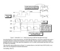
In the attached document in last post, the author mentioned there is a "John Cooley ESNUG effect" (see the attached snapshot), which I have never seen it's been mentioned elsewhere before. Is it real? Why?


Hi,
All the problems mentioned in the above query and replies have been addressed in this paper from sunburst designs.

Speed of Clock ( write and read domains), underflow conditions, avoiding of read when empty, write when full conditions ... are addressed by the paper i the attachment.

I hope it is of use to you

WBR
Lakshman
 

In the attached document in last post, the author mentioned there is a "John Cooley ESNUG effect" (see the attached snapshot), which I have never seen it's been mentioned elsewhere before. Is it real? Why?

What it meant is that because voltage level is hanging around somewhere in the middle, it could be picked as 0 by some inverters(or any logic gates) and picked as 1 by other inverters, so that output of each inverters may be different although logically they must be the same. Remember, the threshold voltage may be different for each inverter and also there are some C and R on the net which may cause a slight fluctuation in the voltage level from point to point, and what's described in the doc could happen and inconsistent values may be captured by the flops down the path if the voltage level doesn't settle by the next clock edge.
 

Thanks lostinxlation. There is a text box in the diagram saying "Clocked signal is initially metastable and is still metastable on the next active clock edge", and the text box is pointing to "bdat1" signal. I don't understand why bdat1 is still in metastable state at that moment.
 

Hi Lakshman

Do you know any other documents in this sunburst site other than the attached one or any othe documents onther than the sunburst site for understanding deciding of FIFO depth for clock domain crossing of data, various clock domain crossing schemes.

Regards
 

Please google the subject. It is a well understood topic.
 

Thanks lostinxlation. There is a text box in the diagram saying "Clocked signal is initially metastable and is still metastable on the next active clock edge", and the text box is pointing to "bdat1" signal. I don't understand why bdat1 is still in metastable state at that moment.

i guess the figure 2 doesn't make sense. First,like you said, bdat1 output should be low during the 2nd cycle since it is forced to be low by a new input data. Second, the indeterminate result on inverter outputs shouldn't be due to the metastability in the 2nd cycle. As long as the metstability doesn't get resolved by the next clock edge, inverter outputs should go indeterminate and the inconsistent data gets captured by the flops down the paths. I don't understand what difference the author is trying to make for between figure 1 and 2..
 
Last edited:

Status
Not open for further replies.

Part and Inventory Search

Welcome to EDABoard.com

Sponsor

Back
Top