jonnybgood
Full Member level 4

Hi,
is this a good explanation for the attached clamping circuit?

C1 will block the DC from affecting the source and will couple the ac signal to the opamp circuit.
a) Vref = 0V
When the inverting input is connected to Ground, this circuit behaves similar to a half wave rectifier. Input signal Vin is seen at the inverting input and the difference between the two inputs is seen inverted at the output of the op amp. When the input signal is at the negative half cycle, the output would have the same peak but positive peak. This enables the diode to conduct and a positive half cycle which cancels out the input negative half putting the output to almost 0Volts. However when the input signal is positive, the output would be negative causing the diode to operate in reverse bias thereby blocking all the output from the op amp and letting the positive input signal to appear at the output. The diode voltage drop will be insignificant in the output as it will be divided by the op amp’s open loop gain.
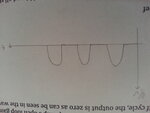
For this half cycle, the output is zero as can be seen in the waveform below;
Vref = +Vref
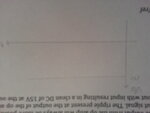
In this scenario, the diode will remain forward biased all the time since the output from the op amp will always be more positive than the input signal. The ripple present at the output of the op amp will cancel out with input resulting in a clean DC of 15V at the output;
Vref = -Vref
When the non-inverting input of the op amp is connected to the negative rail of the op amp, the difference between the inputs would always be negative due to the input signal only being 4Vp-p in this case. Having a output less the input signal at all times would lead to the Diode D1 always reversed bias allowing the input signal to appear almost intact at the output all the time.

is this a good explanation for the attached clamping circuit?

C1 will block the DC from affecting the source and will couple the ac signal to the opamp circuit.
a) Vref = 0V
When the inverting input is connected to Ground, this circuit behaves similar to a half wave rectifier. Input signal Vin is seen at the inverting input and the difference between the two inputs is seen inverted at the output of the op amp. When the input signal is at the negative half cycle, the output would have the same peak but positive peak. This enables the diode to conduct and a positive half cycle which cancels out the input negative half putting the output to almost 0Volts. However when the input signal is positive, the output would be negative causing the diode to operate in reverse bias thereby blocking all the output from the op amp and letting the positive input signal to appear at the output. The diode voltage drop will be insignificant in the output as it will be divided by the op amp’s open loop gain.
For this half cycle, the output is zero as can be seen in the waveform below;

Vref = +Vref
In this scenario, the diode will remain forward biased all the time since the output from the op amp will always be more positive than the input signal. The ripple present at the output of the op amp will cancel out with input resulting in a clean DC of 15V at the output;

Vref = -Vref
When the non-inverting input of the op amp is connected to the negative rail of the op amp, the difference between the inputs would always be negative due to the input signal only being 4Vp-p in this case. Having a output less the input signal at all times would lead to the Diode D1 always reversed bias allowing the input signal to appear almost intact at the output all the time.
