nxing
Advanced Member level 1
Hello
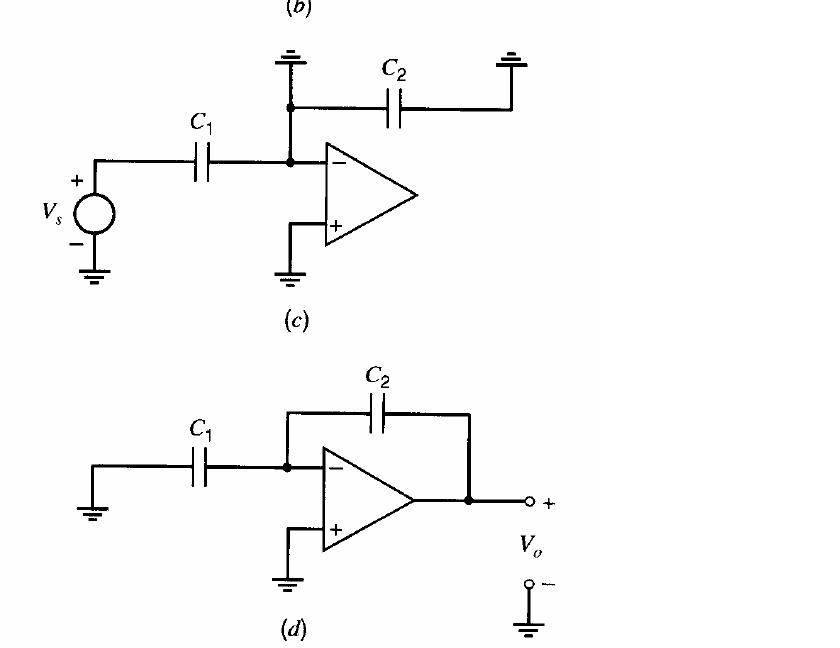
I have a basic question regarding switched-capacitor integrator circuit, look at the attached drawing (from Paul Gray's book, chapter 6). on the top phase (sample phase), I am wondering what's the charge at right plate of C1? I am thinking because it's connected to ground (or any DC voltage), there should be no Charge, if that is the case, why we say at integrating phase (low drawing), the charge will be dumped to capacitor C2?
Thanks,